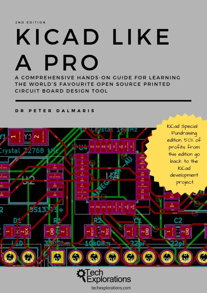
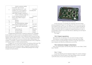
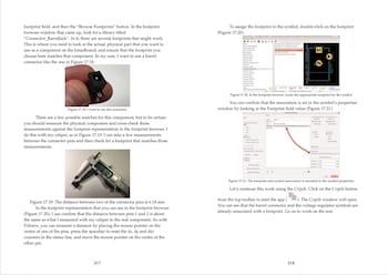
KiCad Like a Pro, 2nd edition
A book for the world's favourite open source printed circuit board design software.
The eBook
The 3rd edition of KiCad Like a Pro is now available.
See the available purchasing options for
KiCad Like a Pro 3e "Special Fundraising Edition".
By purchasing this edition of KiCad Like a Pro 2nd edition, you contribute to the ongoing development of this amazing tool.
Tech Explorations will donate 50% of the profit from all sales of this Special Fundraising edition to the KiCad Project.
Covers the latest Kicad version
The Kicad development team released Kicad 5 in August 2018. This is an almost complete rewrite of version 4. Kicad 5 is full of improvements and new features, including new libraries, a new 3D model viewer, better drawing tools, new symbol and footprint choosers, and new symbol and footprint editors. I wrote this book using Kicad 5.
This ebook was last updated on December 31, 2019, to cover changes in KiCad 5.1.5. It includes several new chapters, recipes, and updates.
Project-based learning
We learn best when we learn in context. Projects provide a context so that learners can understand not just how to do something, but also why it is done in a particular way. This book uses the project-based learning method to help you learn simple and complicated concepts and techniques. Use the book to guide you through these projects, experience the process of creating the boards yourself. Be in control, and be satisfied that you own your learning.
Clarity & reliability
Learning should be a straight-forward, rewarding experience for you. This is why I have filled this book with clear instructions, triple checked and verified. Be illuminated, not confused. And if something still doesn't work, we have your back; simply raise a ticket on our help desk.
Recipes
This book contains numerous recipes of the most useful workflows and activities in Kicad. Find what you need quickly, and get on with your project.
Examples include:
These and many more are all covered, with examples.
Online resources
As a reader of this book, you are welcome to use its online resources:
- A discussion forum where you can interact with the author and other readers
- A repository with all book project files
- An errata form, where you can let the author know about any problems with the book
- A repository of full-resolution images from the book
Multiple formats
This ebook is available in a bundle that contains three formats:
eBook bundle features
Ready to learn?
What will you learn?
Learn practical PCB design skills, built on a solid foundation
Introduction to PCB design
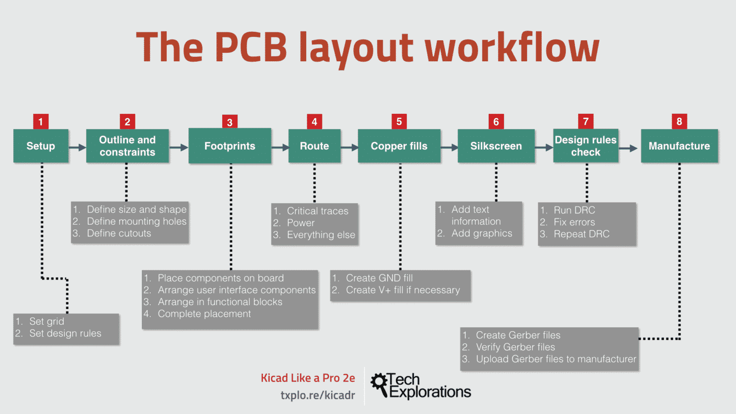
Learn about the basics of PCB design, the design process, the Kicad capabilities. Gain an understanding of the schematic and layout design, and how those are implemented in Kicad. Understand how your board layout is manufactured into a professionally finished product.
Schematic & layout design
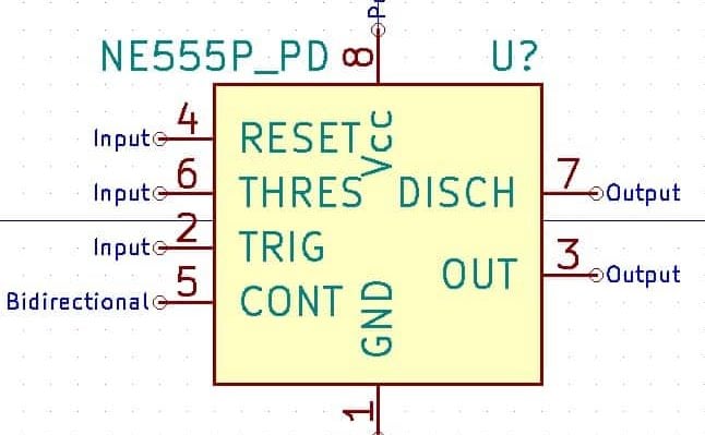
Creating a PCB starts with the schematic design, in which you describe the circuit using symbols. The work concludes with the layout, in which you design the specifications of the board. Learn how to do this in Kicad for circuits and boards of any complexity and size.
Project-based practical skills
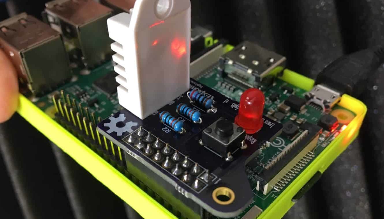
Learn Kicad by working on three real-life projects. With each project, you will learn new skills. Create single, to double and quad-layer boards, manually or automatically routed, with rich features that are both practical and beautiful.
Principles & concepts
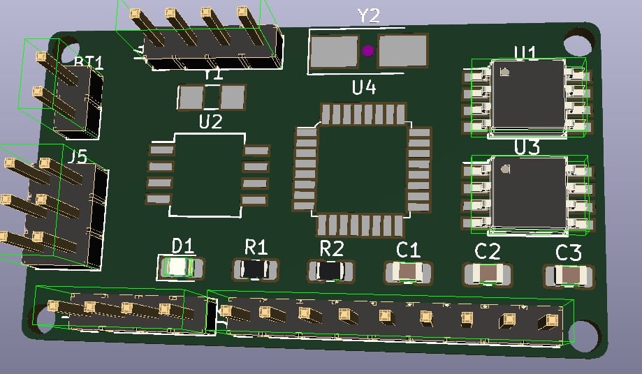
PCB design is engineering and is informed by principles that make designs better in terms of performance, reliability, and manufacturability. This book discusses many of those principles and shows you how to apply them in practice.
Full table of contents
An introduction: Why KiCad?
Part 1: A quick introduction to PCB design
1. What is a PCB?
2. The PCB design process
3. Fabrication
4. Installation
5. Examples of KiCad projects
Part 2: A hands-on tour of KiCad with a very simple project
6. Introduction to this section
7. Start KiCad
8. Schematic design in Eeschema
8.1. The schematic sheet
8.2. Mouse buttons and hotkeys
8.3. Eeschema buttons and menus
9. Layout in Pcbnew
9.1. The user interface
9.2. The layout sheet
9.3. Mouse buttons and hotkeys
9.4. Pcbnew toolbars and menus
Left toolbar
Top toolbar
Right toolbar
Layers manager
Status bar
Menus
Part 3: Design principles and basic concepts
10. About this Part
11. Schematic symbols
12. PCB key terms
12.1. FR4
12.2. Trace
12.3. Pads and holes
12.4. Via
12.5. Annular ring
12.6. Soldermask
12.7. Silkscreen
12.8. Drill bit and drill hit
12.9. Surface mounted devices
12.10. Gold Fingers
12.11. Panel
12.12. Solder paste and paste stencil
12.13. Pick-and-place
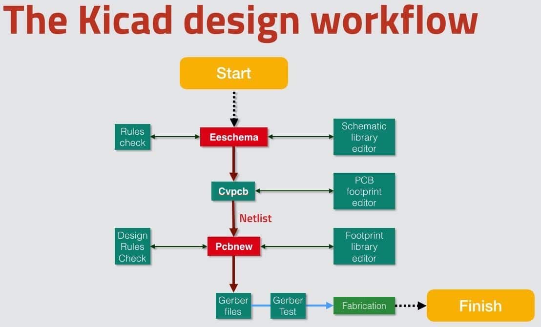
13. Schematic design workflow
13.1. Step 1. Setup
13.2. Step 2. Symbols
13.3. Step 3. Place and annotate symbols
13.4. Step 4. Wire
13.5. Step 5. Nets
13.6. Step 6. Electrical Rules Check
13.7. Step 7. Comments
13.8. Step 8. Netlist
14. PCB layout workflow
14.1. Step 1. Setup
14.2. Step 2. Outline and mechanical constraints
14.3. Step 3. Placement of components
14.4. Step 4. Routing
14.5. Step 5. Copper fills
14.6. Step 6. Silk screen
14.7. Step 7. Design Rules Check
14.8. Step 8. Manufacturing
15. Additional design considerations
15.1. Shape and size
15.2. Layers
15.3. Traces
Length
Angles
Weight
Width
Proximity
Part 4: Projects
16. About this Part
17. Project 1: Design a simple breadboard power supply PCB
17.1. Walk through a simple project
What you will built and list of parts
What you will learn
Project repository
17.2. Schematic design: Eeschema
Step 1: Setup
Step 2: Symbols
Step 3: Arrange, Annotate, Associate
Step 4: Wiring
Step 5: Nets
Step 6: Electrical Rules Check
Step 7: Comments
Step 8: Netlist
17.3. Footprint layout in Pcbnew
Step 1: Setup
Step 2: Outline and constraints
Step 3: Place components
Step 4: Route
Step 5: Copper fills
Step 6: Silkscreen
Step 7: Design Rules Check
Step 8: Manufacture
17.4. Project extensions
18. Project 2: Design a small Raspberry Pi HAT
18.1. What you will built and list of parts
18.2. What you will learn
18.3. Project repository
18.4. Schematic design in Eeschema
Step 1: Setup
Step 2: Symbols
Step 3: Arrange, Annotate, Associate
Step 4: Wiring
Step 5: Nets
Step 6: Electrical Rules Check
Step 7: Comments
Step 8: Netlist
18.5. Footprint layout in Pcbnew
Step 1: Setup
Step 2: Outline and constraints
Step 3: Place components
Step 4: Route
Step 5: Copper fills
Step 6: Silkscreen
Step 7: Design Rules Check
Step 8: Manufacture
19. Project 3: Arduino clone with build-in 512K EEPROM and clock
19.1. Project details
19.2. Project repository
19.3. Schematic design in Eeschema
Step 1: Setup
Step 2: Symbols
Step 3: Arrange, Annotate, Associate
Step 4 and 5: Wiring and Nets
Step 6: Electrical Rules Check
Step 7: Comments
Step 8: Netlist
19.4. Footprint layout in Pcbnew
Step 1: Setup
Step 2 + 3: Outline, constraints and component placement
Step 4: Route
Using the autorouter - two layers
Using the autorouter - four layers
Two layers, or more?
Step 5: Copper fills
Step 6: Silkscreen
Step 7: Design Rules Check
Step 8: Manufacture
Part 5: Recipes
20. Adding a schematic symbol library in Eeschema
21. Adding a footprint library in Pcbnew
22. Using footprint libraries offline
23. Using symbol libraries offline
24. Create a keep-out zone
25. Creating copper fills
26. How to calculate the width of a trace
26. Custom Global Design Rules and changing the width of a trace
27. Create custom net design rules
28. How to add silkscreen text and simple graphics
29. How to add a custom logo to the silkscreen
30. How to manufacture a PCB with Oshpark
31. How to make and test Gerber files
32. How to manufacture a PCB with PCBWay
33. Rounded corners
34. Mounting holes and openings
35. Creating a new component (symbol)
36. Modifying an existing component (symbol)
37. Creating a new footprint - manually
38. Creating a new footprint - using the footprint wizard
39. Modifying an existing footprint
40. Using an autorouter
41. How to create a bill of materials (BoM)
42. How to design a custom page layout
43. How to use hierarchical sheets
44. How to use differential pairs
45. Interactive router
46. Creating unique board edge cuts
47. Using Git for version control
48. Creating a multi-layer PCB
49. How to use buses
50. How to update your schematic and layout (with Git)
51. Starting KiCad apps individually
52. Creating a new version of a PCB without altering the original
53. Making a PCB without a schematic
54. How to set a text editor and why
55. How to install 3D shapes
Who is this book for?
I wrote this book for people with a variety of backgrounds and objectives.
If you are someone with little or no experience in PCB design, you will find this book particularly useful. I took care to make it as gentle as possible for beginners to learn without becoming intimidated by the complexity of the software or the technical language.
About the author
Dr. Peter Dalmaris is an educator, electrical engineer, electronics hobbyist, and Maker.
He is an instructor of DIY electronics and author of several technical books. Peter is also the author of “Maker Education Revolution,” a book about how Making is changing the way we learn and teach in the 21st century.
As a Chief Tech Explorer since 2013 at Tech Explorations, the company he founded in Sydney, Australia, Peter’s mission is to explore technology and help educate the world. Tech Explorations offers educational courses and Bootcamps for electronics hobbyists, STEM students, and STEM teachers.
A lifelong learner, Peter’s core skill lies in explaining difficult concepts through video and text. With over 15 years of tertiary teaching experience, Peter has developed a simple yet comprehensive style in teaching that students from all around the world appreciate.
Our Peace of Mind, No Questions Asked, No Hassle, Money Back Guarantee
My team and I want you to be absolutely happy with your purchase.
We know that you will be spending a lot of time learning, using our books and courses.
Our goal is to help you learn and to enjoy the experience. It is the only way you will come back to learn more, and the only way you will tell your friends about us. Our goal is not frustrate you, annoy you, or to do anything that will spoil your learning experience.
This is why all our courses (except for the Arduino Bootcamp for Teachers) and ebooks purchased from the Tech Explorations website, come with our "Peace of Mind; No Question Asked; No Hassle; Money Back Guarantee."
Our promise is very simple:
If you have purchased any of our books or courses, but you feel that what you got was not worth the money you spent on it, just let us know, and we will refund you the full amount you paid.
You can email raise a ticket in our Help Desk. Just mention which product you want to be refunded, and approximately the date of purchase so we can find your record in our database. If you wish to (this is not required), say why you are not happy with your purchase (this will give us the opportunity to improve).
We will process your refund immediately. If the product is a eBook, you can keep it. If it is a course, we will un-enroll you as part of the refund process.
Because of limits set by our payment gateways, we ask that you request a refund no more than 20 days after your purchase.
Ready to learn?
Please see our refunds policy.

