

Project 2: Tiny Solar Power Supply
In Chapter 8, you built a board of your own, starting from an empty project to a folder of manufacturing files. This chapter builds a second board the same way, as a gentle step up rather than a leap. The circuit is slightly more involved, most of its parts are surface-mount rather than through-hole, and along the way you will meet a few things the breadboard supply did not need. This project introduces 3D models, so you can see the finished board in the round before you order it; a closer look at the design rules KiCad hands you for free; and a handful of new items in the layout, such as your first via, a ground pour stitched down to it, and cross-probing between the two editors. None of this is new territory in the workflow sense. You still take the eight schematic steps and the eight layout steps in the order you already know, and each one leaves the design ready for the next. Keep the one-page checklist from Chapter 5 beside you, and let’s build a second real thing.
The design is not mine. It is a neat circuit called the Tiny Solar Supply, drawn by Clemens Valens for Elektor, and I am rebuilding it in KiCad with only a few small changes of my own. Following someone else’s good schematic is exactly how a great deal of real PCB work begins, so it is a fair and useful thing to practise.
Here is what we are building (Figure 9.1). A power supply that runs from a small solar panel. In daylight the panel charges a rechargeable battery; when the panel falls dark, the board draws on that stored charge instead, so the 3.3 volts it delivers never blink out. That makes it a tidy supply for a low-power project placed on a windowsill, in a garden, or anywhere a wall socket will not reach.
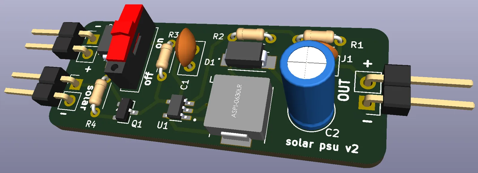
Figure 9.1: The finished tiny solar power supply, rendered from its own design files. The small surface-mount parts sit on top, the three 2-pin headers and the slide switch stand along the edges, and a single board slips into its enclosure on clips.
The circuit is built from a set pile of parts:
- a boost converter1 chip (
U1, an AP3015A), the part that takes a low, wavering input voltage and steps it up to a steady 3.3 volts; - an inductor (
L1) and two Schottky diodes2 (D1,D2), the converter’s working partners that store and steer the energy as it is pumped up; - four resistors (
R1toR4) and three capacitors (C1,C2,C3) that set the output voltage, steady the rails, and bias the control parts; - a small MOSFET3 (
Q1, a 2N7002) that switches the converter on and off automatically, which is the clever heart of the design; - three 2-pin headers, for the solar panel (
J3), the battery (J2), and the 3.3 volt output (J1); - a slide switch (
SW1) to cut the whole thing off by hand.
Let’s have a close look at two aspects of this project. The first is Q1, the part I called the clever heart. I will come back to what it does when we wire it, because it is the one piece of this circuit that is not obvious. The second is simply that most of this board is surface-mount. On the breadboard supply only the USB-C connector was, and every other part was the friendly through-hole kind. Here the boost converter, the inductor, the diodes, and the transistor are all surface-mount, because that is the only sensible way those particular parts come. I have kept the resistors and capacitors as through-hole so the board remains easy to hand-solder, but the surface-mount parts are nothing to worry about. They change nothing about how you design the board, and with a little practice they are every bit as manageable as their through-hole counterparts. If soldering the smallest of them still does not appeal, you can ask the fab to place them for you when you order the boards. For now, designing it is all that matters. Let’s gather the parts.
Footnotes
-
A boost converter is a circuit that raises a DC voltage to a higher one. It works by repeatedly storing energy in an inductor, then releasing it into the output through a diode, switching between the two states fast enough that the output settles at a steady, higher voltage than the input.
U1’sAP3015Achip and theQ1transistor drive that switching automatically, so the board keeps delivering 3.3 volts even as the solar panel’s own voltage rises and falls with the light. ↩ -
A Schottky diode is a diode built from a metal-semiconductor junction rather than the semiconductor-semiconductor junction an ordinary diode uses. That construction switches on and off faster and drops less voltage across itself when conducting, both useful traits in a converter that switches thousands of times a second and cannot afford to waste what little voltage the solar panel gives it. ↩
-
A MOSFET is a transistor that uses a voltage on its gate lead to control the flow of current between its other two leads, drain and source, switching that current on and off rather than amplifying it in the way some other transistors do. That makes it well suited to the job here, where
Q1needs only to decide, cleanly, whether the boost converter runs or rests. ↩