KiCad Like a Pro
4th edition
A book and video course for the world's favorite open source printed circuit board design software.
KiCad Like a Pro eBook is updated for KiCad 9.
The video course is updated for KiCad 9.
This book is the fourth edition of the world's most comprehensive book about the wordl's best open source PCB design application. In the fourth edition of the book, I have made the following changes and additions:
The video course is also updated for KiCad 9. See the curriculum below for more details.
Since KiCad first appeared in the PCB CAD world in 1992, it has gone through 6 major versions and evolved into a serious alternative to commercial products. I have been using KiCad almost daily since version 4 when I published the first edition of KiCad Like a Pro.
In this eBook and video course, I have packed almost everything I have learned as a KiCad user and electronics instructor. I have organized all this knowledge in a way that will make it easy for you to learn KiCad.
The eBook
I wrote this book so that you can use it as a learning guide and as a reference source.
I have tested all examples, descriptions and procedures on KiCad 9.
If you have never used KiCad and have little or no experience in PCB design, you should read this book it in a linear fashion. The first few chapters will give you the fundamental knowledge on which you will build your skill with the projects later in the book.
If you have a good working knowledge of PCB design, but you are new to KiCad, you can learn about the KiCad fundamentals in in the middle of the book, and then continue with the projects.
To get the full benefit of the book, you should consider the complementary video course. This course spans over 30 hours of high-definition video, with detailed explanations and demonstrations of all projects featured in the book. The video lectures capture techniques and procedures that are just not possible to do so in text.
Covers the latest KiCad version
KiCad 9 was published in February 2025.
I wrote this book using KiCad 8 and have updated it for KiCad 9.
Project-based learning
We learn best when we learn in context. Projects provide a context so that learners can understand not just how to do something, but also why it is done in a particular way. This book uses the project-based learning method to help you learn simple and complicated concepts and techniques. Use the book to guide you through these projects, experience the process of creating the boards yourself. Be in control, and be satisfied that you own your learning.
Just learn
Learning should be a straight-forward, rewarding experience for you. This is why I have filled this book with clear instructions, triple checked, verified and illustrated.
Be illuminated, not confused.

Looking for a sample?
View a free section the web version of this book.
Recipes
This book contains numerous recipes of the most useful workflows and activities in KiCad. Find what you need quickly, and get on with your project.
Examples include:
These and many more are all covered, with examples.
Online resources
As a reader of this book, you are welcome to use its online resources:
Multiple formats
This eBook is available in a bundle that contains three formats:
eBook features
The video course
This video course will teach you KiCad so that you can use it in your commercial or hobby projects. It takes a practical approach to learning that combines "how-to" content with complete start-to-finish PCB projects.
If you are new to PCB design, this course will help you get started from the ground level. If you are an experienced PCB designer, this course will help you transition to KiCad from another tool or an earlier version of Kicad.
To get the full benefit of the video course, you should consider the complementary eBook. This eBook contains more than 1,000 pages and 1,000 images, with detailed step-by-step instructions from every lecture in the video course. You can use the eBook as a quick reference source as well as a learning guide to support the video course.
Follows the methodology and content of the book
The video course is designed as the perfect companion of the eBook. Its adds video to enhance your learning.
Perfect for hands-on "seeing is believing" learning
The combination of video and text is powerful. Video is perfect for hands-on "seeing is believing" learning. It's almost as good as looking over my shoulder as I design a PCB.
You can see every click, every select, every key typed, in real time. But the book contains the detail and the depth that the video doesn't.
Plus, the eBook is perfect as a quick resource. You can search and jump to any part of the eBook in seconds, and find the answer you are looking for that is relevant to your project
Content
The course contains all of the projects and recipes of the book, in video.
Keep your book handy for quick referencing.
The book plus the course give provide you with an amazing learning resource for KiCad.
Study guide
What is this course about?
Sample lecture
Online resources
As a student of this course, you are welcome to use its online resources:
Course features
Ready to learn?
You can enroll to our courses in one of three options: Solo, and Community. For more information, please see this explainer page.
ebook ONLY
eBook only, in four formats
SOLO
Once-off payment, best for self-sufficient learners on a budget.
...
Once-off.
COMMUNITY
Best for the social learner: become a member of the course community.
...
Once-off.
Course + eBook
Get the lot, with the full video course and eBook resources
BUNDLE SOLO
Once-off payment, best for self-sufficient learners on a budget.
...
Once-off.
BUNDLE COMMUNITY
Best for the social learner: become a member of the course community.
...
Once-off.
course ONLY
Get the video course only
SOLO
Once-off payment, best for self-sufficient learners on a budget.
...
Once-off.
COMMUNITY
Best for the social learner: become a member of the course community.
...
Once-off.
Consider a subscription
Did you know, you can get a subscription for immediate access to this and 20+ of our courses. All for a low monthly payment, cancel anytime.
Do you prefer to learn on Udemy?
On Udemy you will find all of the Tech Explorations courses at the lowest possible price.
Each course is individually priced by Udemy based on your location. We don't have control of the price on Udemy and so we can't display it on this page.
Click on the button below to open a new window where you can see the price of this course on the Udemy website.
Please see our refunds policy.
What some of our students say
Thanks for saving me during the COVID pandemic with the book and the course!
Hi Peter,
Well is all started in March 2020 with the pandemic. A little history first. I have been teaching Electrical Engineering for over 30 years and when the pandemic hit we all had to leave campus and head home to zoom classes. Just then my lab technician sent out and email about free PCB classes. I haven’t done much PCB work in many years and thought it was about time to get back into it. Well I tried the “free course” and it was extremely rigorous and all 300 participants could choose what EDA tool to use (Altrium, Eagle, KiCad,etc…). I chose the KiCad section along with 147 participants learning KiCad. It was a major up hill climb but I was determined to complete it. The “free” course materials went over very general topics of the entire PCB process, which I was very grateful for and to learn from, but it was up to each participant to “master” their EDA tool.
I saw and went through every YouTube video I could find and learned the basics of KiCad but it still wasn’t enough to complete the “free” course. Then I ran across your book and it was a Godsend! I immediately jumped in and went all the way through the 3 projects. If it wasn’t for your book, I probably wouldn’t have completed the “free” course. Only 6 out of 147 participants in the KiCad section completed the course and received the final manufactured PCB. That was back in last September 2020.
I then went back to zooming my classes over the Fall 2020 and Spring 2021 semesters and when the Spring semester was completed, I decided to get back into the PCB swing of things and signed up for your course.
As an electrical engineer and an academic (34 years) I was amazed at the organization, thoroughness, attention to detail, and professional presentation your course was designed to be. It was an absolute pleasure working through all of the projects, each one increasing the both the level of complexity and the learning skills acquired. Getting the boards manufactured and sent back completely functional felt like a “feather in the cap for me!”
I am currently signing up for other Tech Explorations courses and can’t wait to dive in to them like the KiCad course.
Many, many thanks for keeping me sane and productive during the pandemic!
Dr. John J Helferty
Temple University
Electrical and Computing Engineering Department
Excellent library of documentation for micropython
This course is composed of dozens of bite sized projects for the ESP32 using MicroPython. Each project has an excellent header with links to a wealth of documentation about the concepts of the project. It’s one of the best collections of documentation resources I have seen for working with the ESP32. I highly recommend this course.
Good course.
I had tried KiCad before, on my own, and didn’t end up using it – used Eagle instead. I wanted to try KiCad again but thought some instruction might be helpful. My first impression may have been that the course was slow moving, but after doing a significant part of it, I realize that Peter’s presentation was thorough with suitable repetition for retention. I am understanding the workflow, unlike my previous attempt at KiCad, and retaining the information well. Good examples for working through.
An oasis in a desert of wanna be's
OMG ! Peter is an awesome teacher. He is amaaazingly thorough, clear, and concise. I got the “KiCad Like a Pro” book and then, before I started the book, got the video course. The video course is cheap at twice the price! I’m very critical and usually don’t write reviews, but this course was so good, I had to let everyone know. Kudos Peter, and thanks.
What will you learn?
Learn practical PCB design skills, built on a solid foundation
Introduction to PCB design

Learn about the basics of PCB design, the design process, the KiCad capabilities. Gain an understanding of the schematic and layout design, and how those are implemented in KiCad. Understand how your board layout is manufactured into a professionally finished product.
Schematic and layout design

Creating a PCB starts with the schematic design, in which you describe the circuit using symbols. The work concludes with the layout, in which you design the specifications of the board. Learn how to do this in KiCad for circuits and boards of any complexity and size.
Project-based practical skills

Learn KiCad by working on three real-life projects. With each project, you will learn new skills. Create single, to double and quad-layer boards, manually or automatically routed, with rich features that are both practical and beautiful.
Design principles & concepts

PCB design is engineering and is informed by principles that make designs better in terms of performance, reliability, and manufacturability. This book discusses many of those principles and shows you how to apply them in practice.
Full table of contents
Book
Updated for KiCad 9
VOLUME 1
Part 1.1: Introduction
What is a PCB?
The PCB design process
Fabrication
Get KiCad for your operating system
Example KiCad projects
Part 1.2: Getting started with KiCad
Introduction
KiCad Project Manager (main window)
Overview of the individual KiCad apps
Paths and Libraries
Create a new project from scratch
Create a new project from a template
KiCad on Mac OS, Linux, Windows
KiCad 8
KiCad 9
Part 1.3: Project - A hands-on tour of KiCad - Schematic Design
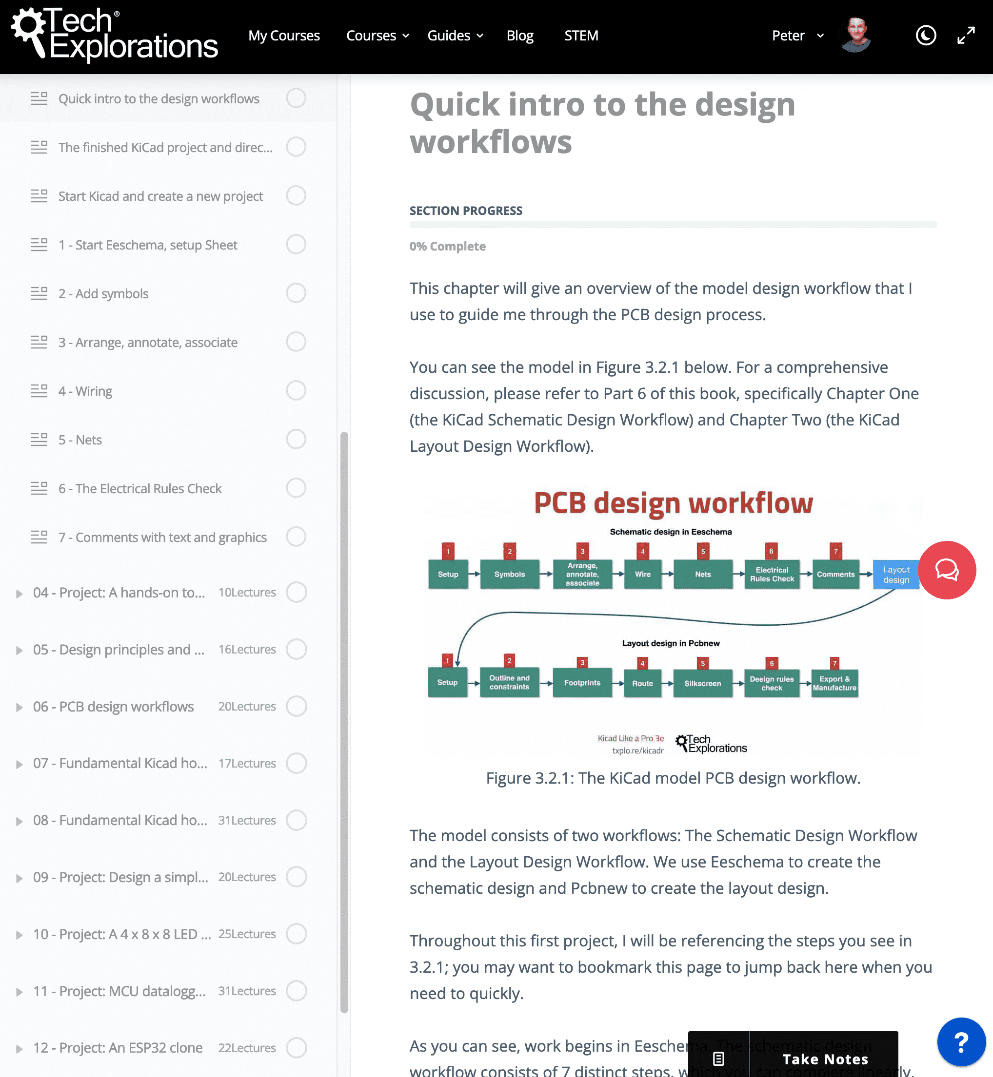
Introduction to schematic design and objective of this section
Design workflows summary
The finished KiCad project and directory
Start Kicad and create a new project
1 - Start Eeschema, setup Sheet
2 - Add symbols
3 - Arrange, annotate, associate
4 - Wiring
5 - Nets
6 - The Electrical Rules Check
7 - Comments with text and graphics
Part 1.4: Project- A hands-on tour of KiCad - Layout
Introduction to layout design and objective of this section
1 - Start Pcbnew, import footprints
2 - Outline and constraints (edge cut)
3 - Move footprints in place
4 - Route (add tracks)
5 - Refine the outline
6 - Silkscreen (text and graphics)
7 - Design rules check
8 - Export Gerbers and order
The manufactured PCB
Part 1.5: Design principles and PCB terms
Introduction
Schematic symbols
PCB key terms
FR4
Traces
Pads and holes
Via
Annular ring
Soldermask
Silkscreen
Drill bit and drill hit
Surface mounted devices
Gold Fingers
Keep-out areas
Panel
Solder paste and paste stencil
Pick-and-place
Part 1.6: PCB design workflows
The KiCad Schematic Design Workflow
Schematic Design Step 1: Setup
Schematic Design Step 2: Symbols
Schematic Design Step 3: AAA (Arrange, Annotate, Associate)
Schematic Design Step 4: Wire
Schematic Design Step 5: Nets
Schematic Design Step 6: Electrical Rules Check
Schematic Design Step 7: Comments and Graphics
The KiCad Layout Design Workflow
Layout Design Step 1: Setup
Layout Design Step 2: Outline and constraints
Layout Design Step 3: Place footprints
Layout Design Step 4a: Route
Layout Design Step 4b: Copper fills
Layout Design Step 5: Silkscreen
Layout Design Step 6: Design rules check
Layout Design Step 7: Export & Manufacture
Part 1.7: Fundamental Kicad how-to: Symbols and Schematic Editor
Introduction
Left toolbar overview
Top toolbar overview
Right toolbar overview
Schematic editor preferences
How to find a symbol with the Chooser
How to find schematic symbols on the Internet
How to install symbol libraries in bulk
How to create a custom symbol
How to associate a symbol with a footprint
Net labels
Net classes
Hierarchical sheets
Global labels
Hierarchical labels and import sheet pin
Electrical rules and customization
Bulk editing of schematic elements
Part 1.8: Fundamental Kicad how-to: Footprints and PCB Editor
Introduction
Left toolbar
Top toolbar
Top toolbar Row 1
Top toolbar Row 2
Right toolbar
Right toolbar main buttons
Right toolbar - Appearance
Layout editor preferences
Board Setup
Board Setup - Board Stackup
Board Setup - Text & Graphics
Board Setup - Design Rules and net classes
Board Setup - Design Rules - Custom Rules and violation severity
How to find and use a footprint
Footprint sources on the Internet
How to install footprint libraries
Filled zones
Keep-out zones
Interactive router
Length measuring tools
Bulk editing
Create a custom footprint, introduction
Create a new library and footprint
Create a footprint, 1, Fabrication layer
Create a footprint, 2, Pads
Create a footprint, 3, Courtyard layer
Create a footprint, 4, Silkscreen layer
Use the new footprint
Finding and using a 3D shape for a footprint
How to export and test Gerber files
Part 1.9: Project - Design a simple breadboard power supply PCB
Introduction
Schematic
1 - Setup
2 - Symbols
2 - Edit Component values
3 - Arrange, Annotate
3 - Associate
4 - Wiring
5 & 6 - Nets and Electrical Rules Check
7 - Comments
Layout
1 - Setup
2 - Outline and constraints
3 - Place footprints
2 - Refine the outline
4 - Route
5 - Copper fills
6 - Silkscreen
7 - Design Rules Check
8 - Export and Manufacture
Finding and correcting a design defect
Fix the schematic
Fix the layout
Part 1.10: Recipes
Edit Text & Graphics Properties
Pack & Move footprints
Interactive router modes
Create a custom silkscreen or copper graphic
Bill of Materials
Build-in BOM in the PCB editor
Build-in BOM in schematic editor
A plug-in for BOM
Grid Overrides
Edit Teardrops
Buses
Field name templates
Plugin and Content Manager: Plugins
Plugin and Content Manager: Libraries
Plugin and Content Manager: Themes
PCB editor origins
Edit Track & Via Properties (PCB editor)
Change a symbol in bulk
Change a footprint in bulk
Part 1.11: PCB manufacturing and tools
NextPCB KiCad Quote and Order plugin
NextPCB Gerber Viewer and Analysis tool
NextPCB PCB Design Analysis Software for Manufacturability
NextPCB KiCad DFM analysis plugin
VOLUME 2
Part 2.1: Project - Tiny Solar Power Supply
Introduction
Schematic
1 - Setup
2 - Symbols
2 - Edit Component values
3 - Arrange, Annotate, Associate
4 - Wiring
5 & 6 - Nets and Electrical Rules Check
7 - Comments
Layout
1 - Setup
2 & 3 - Placement and outline
4 - Route
2 - Refine the outline
5 - Copper fills
6 - Silkscreen
7 - Design Rules Check
Two more things: 3D models and mounting holes
8 - Export and Manufacture
Part 2.2: Project - A 4 x 8 x 8 LED matrix array
Introduction
Schematic design
1 - Setup
2 - Symbols
3 - Arrange, Annotate
3 - Associate
4 - Wiring
5 - Nets
6 - Electrical Rules Check
7 - Comments
Last-minute edits
Layout design editing
1 - Setup
2 - Outline and constraints
3 - Place components
2 - Refine outline
3 - Move footprints
4 - Route
4 - Copper fills
5 - Silkscreen
6 - Design Rules Check
7 - Manufacture
Bonus - 3D shapes
Bonus - Found a bug in the schematic! (and fix)
Assembled PCB
Part 2.3 : Project - MCU datalogger
Project - Introduction
Create the new project and Git repository
Schematic design
Schema 1 - Setup
Schema 2 - Symbols
Schema 2 - Sheet two
Schema 3 - Arrange, Annotate
Edit component values
Schema 3 - Associate
Schema 4 - Wiring of sheet 1
Schema 4 - Wiring of sheet 2
Schema 5 - Nets
Schema 6 - Electrical Rules Check
Schema 7 - Comments
Create the 2-layer branch in Git
Layout design
Layout 1 - Setup
Layout 2 - Outline and constraints
Layout 3 - Place components
Layout 2 - Outline refinement
Layout 4 - Route
Layout 4 - Copper fills
Layout 4 - Routing improvements
Layout 5 - Silkscreen
Layout 6 - Design Rules Check
Layout 7 - Manufacture
3D shapes
Merge 2-layer branch to main
Design 4 Layer PCB in new Git branch
Four-layer PCB routing
Four-layer PCB manufacturing
Updating layout from changes to the schematic with Git
Finding and correcting a design defect
Fix the schematic
Fix the 2 layer PCB layout
Fix the 4 layer PCB layout
Part 2.4 : Project - An ESP32 clone
Project - Introduction
Schematic design
Schema 1 - New KiCad project and Schematic Setup
Schema 2 - Symbols
Schema 3 - Annotate and set component values
Schema 3 - Arrange
Schema 3 - Associate
Schema 4 - Wiring
Schema 5 - Nets and Net Classes
Schema 6 - Electrical Rules Check
Schema 7 - Comments
Layout design
Layout 1 - Setup
Layout 2 - Outline and constraints
Layout 3 - Place components
Layout 2 - refine outline and DRC errors
Layout 4 - Route
Layout 4 - Copper fills and keep out areas
Layout 5 - Silkscreen
Layout 4 - Routing improvements
Layout 6 - Design Rules Check
Layout 7 - Manufacture
3D shapes
Finding and correcting a design defect
Fix the schematic
Fix the layout
Part 2.5: Recipes
Interactive delete
Find and Replace (Schematic editor)
Text variables
Board Setup - pre-defined sizes for tracks and vias
Board Setup - Design rules violation severity
Board Setup - Custom design rules
Schematic Setup - Electrical Rules and violation severity
Schematic Setup - Electrical Rules and Pin conflicts map
Import components from Snapeda
The Freerouting autorouter
Freerouting plugin installation and operation
Using Freerouting
Autorouting process and customisation
PCB editor Inspection menu
Single track and differential pair routing
Track length tuning
Differential pair skew tuning
The footprint wizard
Pin and wire highlighter tool
KiCad project management with Git
Install Git
Git configuration
Create a new KiCad project Git repository
How to ignore files
Basic Git commands: add, commit
Basic Git commands: branch
Basic Git commands: merge
Sharing your KiCad project on GitHub
Customize the editor color scheme
Import an EAGLE, Altium, or Cadstar schematic
The circuit simulator
Prepare the circuit for simulation
Configure the simulator
Simulate
KiCad project templates
Using a system project template
Create a user project template
Share projects and configurations with others
Calculate the width of a trace
Design a custom schematic sheet
Python scripting API
Kicad 9 Jobsets
Kicad 9 Bezier Curve Tool in All Editors
Kicad 9 Zone Manager
Kicad 9 Design Blocks
Kicad 9 Autorouter attempt finish
Kicad 9 Multiple Track Drag
Kicad 9 Pad Stacks with Different Copper Shapes
Kicad 9 3D model export improvements
Kicad 9 Precision Positioning Tool
Kicad 9 Tables
Kicad 9 Selection filter in the schematic editor
Kicad 9 Component classes
Video
Updated for KiCad 9
01 - Introduction
Why KiCad?
What is this course about?
Study guide TE
Study guide UD
Contribute to KiCad
Software and Hardware requirements
KiCad 9 update lectures
02 - Getting started with PCB design
What is a PCB?
The PCB design process
Manufacturing
Supported operating systems and installation
Example project
03 - Getting started with KiCad
Introduction (what is this section about?)
KiCad project manager
Overview of the individual KiCad apps
Paths and Libraries
Create a new project from scratch
Create a new project from a template
Kicad on Mac OS, Linux, Windows (replace)
04 - Project: A hands-on tour of KiCad - Schematic Design
Introduction to schematic design and objective of this section
Quick intro to the design workflows
The finished KiCad project and directory
Start KiCad and create a new project
1 - Start Eeschema, setup Sheet
2 - Add symbols
3 - Arrange, annotate, associate
4 - Wiring
5 - Nets
6 - The Electrical Rules Check
7 - Comments with text and graphics
05 - Project: A hands-on tour of KiCad - Layout
Introduction to layout design and objective of this section
1 - Start Pcbnew, import footprints
2 - Outline and constraints (edge cut)
3 - Move footprints in place
4 - Route (add tracks)
5 - Refine the outline
6 - Silkscreen (text and graphics)
7 - Design rules check
8 - Export Gerbers and order
The manufactured PCB
06 - Design principles and PCB terms
Design principles and basic concepts - Introduction
Schematic symbols
PCB materials and FR4
Traces
Keep-out areas
Pads and holes
Via
Annular ring
Solder mask
Silkscreen
Drill bit and drill hit
Surface mounted devices
Gold Fingers
Panel
Solder paste and paste stencil
Pick-and-place
07 - Design workflow and considerations
Introduction to the Schematic Design Workflow
Schematic Design Step 1: Setup
Schematic Design Step 2: Symbols
Schematic Design Step 3: AAA (Arrange, Annotate, Associate)
Schematic Design Step 4: Wire
Schematic Design Step 5: Nets
Schematic Design Step 6: Electrical Rules Check
Schematic Design Step 7: Comments and Graphics
Introduction to the PCB Layout Workflow
Layout Design Step 1: Setup
Layout Design Step 2: Outline and constraints
Layout Design Step 3: Place footprints
Layout Design Step 4: Route
Layout Design Step 5: Silkscreen
Layout Design Step 6: Design rules check
Layout Design Step 7: Export & Manufacture
Shape and size
Layers
Traces
08 - Fundamental KiCad how-to: Symbols and Eeschema
About this section
Left menu bar overview
Top menu bar overview
Right menu bar overview
Schematic editor preferences
How to find a symbol with the Chooser
How to find schematic symbols on the Internet
How to install symbol libraries in bulk
How to create a custom symbol
How to associate a symbol with a footprint
Net labels
Net classes
Hierarchical sheets
Global labels
Hierarchical labels and import sheet pin
Electrical rules and customization
Bulk editing of schematic elements
09 - Fundamental KiCad how-to: Footprints and Pcbnew
About this section
Left menu bar overview
Top menu bar overview Part 1
Top menu bar overview Part 2
Right menu bar overview
Right menu bar overview - Appearance
Layout editor preferences (Preferences window, PCB Editor)
Board Setup - Board Stackup
Board Setup - Text & Graphics
Board Setup - Design Rules - Constraints, sizes, classes
Board Setup - Design Rules - Custom Rules and violation severity
How to find and use a footprint
Footprint sources on the Internet
How to install footprint libraries
Filled zones
Keep-out zones
Interactive router
Length measuring tools
Bulk editing
Create a custom footprint, introduction
Create a custom footprint, 1, Fabrication layer
Create a custom footprint, 2, Pads
Create a custom footprint, 3, Courtyard layer
Create a custom footprint, 4, Silkscreen layer
Finding and using a 3D shape for a footprint
How to export and test Gerber files
10 - Project: Design a simple breadboard power supply PCB
Project - Introduction
Schema 1 - Setup
Schema 2 - Symbols
Edit Component values
Schema 3 - Arrange, Annotate
Schema 3 - Associate
Schema 4 - Wiring
Schema 5 & 6 - Nets and Electrical Rules Check
Schema 7 - Comments
Introduction to layout editing
Layout 1 - Setup
Layout 2 - Outline and constraints
Layout 3 - Place components
Layout 2 supplemental - Refine outline
Layout 4 - Route
Layout 5 - Copper fills
Layout 6 - Silkscreen
Layout 7 - Design Rules Check
Layout 8 - Export and Manufacture
11 - Project: Tiny Solar Power Supply
Introduction
Download the circuit PDF from Elektor
1 - Schematic Setup
2 - Schematic Symbols
2 - Edit Component values
3 - Arrange, Annotate, Associate
4 - Wiring
5 & 6 - Nets and Electrical Rules Check
7 - Comments
Layout
1 - Setup
2 & 3 - Placement and outline
4 - Route
2 - Refine the outline
5 - Copper fills
6 - Silkscreen
12 - Project: A 4 x 8 x 8 LED matrix array clock
Project - Introduction
Schema 1 - Setup
Schema 2 - Symbols
Schema 3 - Arrange, Annotate
Schema 3 - Associate
Schema 4 - Wiring
Schema 5 - Nets
Schema 6 - Electrical Rules Check
Schema 7 - Comments
Schema - Last-minute edits
Layout 1 - Setup
Layout 2 - Outline and constraints
Layout 3 - Place components
Layout 2 supplemental - Refine outline
Layout 3 supplemental - Move footprints to back layer
Layout 4 - Route
Layout 4 - Copper fills
Layout 5 - Silkscreen
Layout 6 - Design Rules Check
Layout 7 - Manufacture
Bonus - 3D shapes
Bonus - Found a bug in the schematic! (and fix)
The assembled and working PCB
13 - Project: MCU datalogger with build-in 512K EEPROM and clock
Project - Introduction
Create the new project and create new Git repository
Schema 1 - Setup
Schema 2 - Symbols
Schema 2 - Create a second sheet for the connectors
Schema 3 - Arrange, Annotate
Edit Component values
Schema 3 - Associate
Schema 4 - Wiring of sheet 1
Schema 4 - Wiring of sheet 2
Schema 5 - Nets
Schema 6 - Electrical Rules Check
Schema 7 - Comments
Git, setup in a 2-layer PCB branch
Layout 1 - Setup
Layout 2 - Outline and constraints
Layout 3 - Place components
Layout 2 - Outline refinement
Layout 4 - Route
Layout 4 - Copper fills
Layout 4 - Routing improvements
Layout 5 - Silkscreen
Layout 4 - Fix new routing violations
Layout 6 - Design Rules Check
Layout 7 - Manufacture
3D shapes
Merge 2-layer branch to main
Alternative routing: 4 Layer PCB in new Git branch
Four-layer PCB routing
Four-layer PCB manufacturing
Updating layout with changes to the schematic with Git and gitattributes
14 - Project: An ESP32 clone
Project - Introduction
Schema 1 - New KiCad project and Schematic Setup
Schema 2 - Symbols
Schema 3 - Annotate and set component values
Schema 3 - Arrange
Schema 3 - Associate
Schema 4 - Wiring
Schema 5 - Nets and Net Classes
Schema 6 - Electrical Rules Check
Schema 7 - Comments
Layout - Introduction
Layout 1 - Setup
Layout 2 - Outline and constraints
Layout 3 - Place components
Layout 2 supplemental - refine outline
Layout 4 - Route
Layout 4 - Copper fills and keep out areas
Layout 5 - Silkscreen
Layout 4 - Routing improvements
Layout 6 - Design Rules Check
Layout 7 - Manufacture
3D shapes
15 - Recipes
How to create a custom graphic
How to change a footprint in Pcbnew in bulk
Text variables
How to import symbols, footrpints and 3D shapes from Snapeda
How to create custom sizes for tracks and vias
The Freerouting autorouter introduction
Install and start FreeRouting on MacOS
Install and start FreeRouting on Linux Kubuntu
Install and start FreeRouting on Windows
How to use the Freerouting autorouter 2-layer example
How to use the Freerouting autorouter 4-layer example
KiCad project management with Git
Getting started with Git in KiCad
Sharing your KiCad project on GitHub
Field name templates
Router modes: highlight collisions - shove - walk around
The footprint wizard
Pcbnew Inspection menu
Single track and differential pair routing
Track length tuning
Differential pair skew tuning
Pin and wire highlighter tool
How to customize the editor color scheme
Pcbnew Origins
How to import an EAGLE, Altium, or Cadstar project
How to generate a BOM (Bill of Materials)
The KiCad circuit simulator
How to import a KiCad 5 project
How to create a KiCad project template
Archive/unarchive and share a project
Vias and blind/buried/micro vias
Team KiCad development with Cadlab.io
The Python API
The Plugin and content manager
Polygon arcs
How to make a global text or graphic change in Pcbnew
16 - KiCad 9 new features and updates
Introduction to this section
Jobsets
Bezier curve tool in all editors
Zone manager
Design blocks
Autorouter attempt finish
Multiple track drag
Pad stacks with different copper shapes
3D model export improvements
Precision positioning tool
Tables
Selection filter in the schematic editor
Component classes
17 – KiCad 7 new features and changes
Custom fonts, text boxes and hyperlinks
Wires at 45 degree angles
New drawing primitives
Inverse text objects in PCB
Plugin and Content Manager
Orthogonal dragging
Drag & Drop
PDF export improvements
Search panel
Properties panel
Automatic zone filling
PCB Layout Tool Enhancements – Unroute Selected
PCB Layout Tool Enhancements – Automatically Complete Trace Route
Improved Pack & Move footprints
Command Line Interface
Simulation model editor
Off Grid ERC Warnings
PCB editor footprint consistency and ignored DRC tests
New net class assignment UI
18 - (Legacy) Getting started with KiCad
KiCad 7 project manager
KiCad 6 Project Manager (main window)
Kicad 7 on Mac OS, Linux, Windows
Kicad 6 on Mac OS, Linux, Windows
Major Differences between KiCad 6.0 and 5.0
KiCad 7 vs 6: Schematic editor
KiCad 7 vs 6: Symbol editor
KiCad 7 vs 6: PCB editor
KiCad 7 vs 6: Footprint editor
KiCad 7 vs 6: Gerber viewer
KiCad 7 vs 6: Image converter
KiCad 7 vs 6: Calculator tools
KiCad 7 vs 6: Drawing sheet editor
KiCad 7 vs 6: Plugin and Content Manager
19 - Conclusion
Congratulations!
Who is this book for?
I wrote this book for people with a variety of backgrounds and objectives.
If you are someone with little or no experience in PCB design, you will find this book particularly useful. I took care to make it as gentle as possible for beginners to learn without becoming intimidated by the complexity of the software or the technical language.


About the author
Dr. Peter Dalmaris is an educator, electrical engineer, electronics hobbyist, and Maker.
He is an instructor of DIY electronics and author of several technical books. Peter is also the author of “Maker Education Revolution,” a book about how Making is changing the way we learn and teach in the 21st century.

As a Chief Tech Explorer since 2013 at Tech Explorations, the company he founded in Sydney, Australia, Peter’s mission is to explore technology and help educate the world. Tech Explorations offers educational courses and Bootcamps for electronics hobbyists, STEM students, and STEM teachers.
A lifelong learner, Peter’s core skill lies in explaining difficult concepts through video and text. With over 15 years of tertiary teaching experience, Peter has developed a simple yet comprehensive style in teaching that students from all around the world appreciate.
Free course companion and sample
This PDF file is a companion to the KiCad Like a Pro 3e video course*. This download is free for any student of the course.
It contains chapters that you will need for the study of the course content.
* I will update this companion PDF when KiCad Like a Pro 4e video course is published. You will receive the new companion PDF when it is ready.

© 2025 Tech Explorations