KiCad 6 had arrived! (updated December 26, 2021).
KiCad 6.0 is expected to arrive in the second or third quarter of 2021 and is the first major release since 2018. I took much of January to "play" with the KiCad nightly builds, tagged "KiCad 5.99", which will eventually become KiCad 6.0.
In this article, I document many of the most important changes that the KiCad developers have introduced to KiCad 6, including numerous "under the hood" improvements, and new productivity features in the front end.
Enjoy!
-- Peter Dalmaris, (originally published in January 2021, updated December 2021)

KiCad is arguably the world’s best open-source printed circuit board CAD program.
It’s been around for almost 30 years. Its community has been growing steadily both in terms of end-users and contributors.
KiCad’s importance as a fully-featured alternative to closed-sources PCB design tools has grown since version 4 came out in 2015. That’s about the time that I committed to using KiCad, after playing around with other commercial and open-source alternatives. I was so impressed with KiCad that I decided to teach others how to use it.
I’m pleased with my choice. As an educator and electronics hobbyist, KiCad has everything I need, without the limits.
When KiCad 5 came out in July 2018, KiCad presented an image of maturity. In my opinion, KiCad 5 was a significant milestone in its history because it signified a new approach to the development of the tool.
The core development team, composed of members that give most of their time to the project, is supported by community donations and CERN.
KiCad 5 raised KiCad as a serious contender in the PCB CAD space. KiCad 5 was powerful enough to be used in corporate engineering departments as well as by hobbyists.
After more than two years since the publication of version 5, version 6 is visible in the horizon. I expect that KiCad 6.0 will become a reality sometime in the second or (more likely) third quarter of 2021.
I wanted to take a deep dive in KiCad 6 and report on my findings in this article. As I am writing this post, it is middle of January 2021, a few months after a feature freeze was declared in late 2020.
After months of playing with the nightly builds containing the work in progress towards KiCad 6.0, I decided that it was time to take a closer look.
I felt confident that my findings would be useful to anyone wondering about KiCad 6.
In this article, I document the most important new and updated features coming in KiCad 6.0. In many cases, I make a Kicad 6 vs KiCad 5 comparison so that you can see these changes in context.
For my testing, I use the nightly build of KiCad, which is currently labelled “5.99”. The nightly development builds are snapshots of the development branch of the KiCad repository.
I’m running KiCad 5.99 on an Ubuntu 20.04 virtual machine.
If you want to learn how to install the nightly build, look for instructions at the end of this article.
I am comparing KiCad 5.99 (which will morph into KiCad 6 later this year) with KiCad 5.1.9 running on an Ubuntu 18.04 virtual machine.
Please note that I will be using the designation “KiCad 6” in this article, even though I did my testing on the KiCad nightly release designated “KiCad 5.99”. During this article’s writing, I updated my copy of KiCad 5.99 almost daily to make sure I worked with the latest available code.
If you think I missed an important KiCad 6 feature, change, or improvement, or if you found an error in this article, please let me know.
Help me by using the comments box at the bottom of this page and I will update the article right away.
Extra kudos for you if your comment is clear, consise, and enhanced with images/video or links to original documentation.
Ready to learn KiCad?

Learn the world's favorite open-source PCB design tool with the world's most comprehensive course
KiCad Like a Pro, 3rd edition is available as a video course or as an eBook.
With KiCad Like a Pro 3e you will learn how to design printed circuit boards using KiCad 6.
Choose the version that fits best with your style of learning, or get both to get the full benefit of the video demos plus the details of the eBook.
When you complete KiCad Like a Pro 3e, you'll be able to use KiCad to design and manufacture multi-layer PCBs with highly integrated components and a professional-looking finish.
Work through five projects that give many opportunities to learn and practice all of KiCad's important features.
KiCad Like a Pro 3e contains full sections dedicated to PCB and design principles and concepts. These ensure that you will master the fundamentals so that your PCB project are awesome.
If you are someone who is interested in designing PCBs using KiCad, or moving to KiCad from another CAD application, then KiCad Like a Pro, the video course and eBook, is for you.
KiCad 6 impressions in a nutshell
KiCad 6 includes several big changes and many smaller ones.
Many of those changes are under the hood, designed to improve reliability and performance and set the stage for the future.
Of course, there are numerous changes in the front end, the user interface, that will impact how you interact with KiCad.
New file format
In my opinion, the most significant changes are the ones we can’t see.
At the top of these changes, you’ll find the introduction of a new format for the schematic files, which uses the S-Expressions notation. S-Expressions can represent data in a tree structure format as a nested list. The new file format makes schematic and layout file human-readable, and, just as important, much easier to manipulate programmatically using Python or other programming languages.
S-Expression notation is not new to KiCad. Layout (".kicad_pcb") and footprint files (".kicad_mod") have used S-Expression notation in KiCad 5. But with KiCad 6, the transition is complete.
Bellow, you can see a side-by-side comparison of the same schematic file section. KiCad 6 on the left, KiCad 5 on the right. In both cases, the text describes a PWR symbol with designation “PWR07”.

KiCad 6, Eeschema, S-Expression notation schematic file (partial)

KiCad 5, Eeschema, notation schematic file (partial)
KiCad 5, Eeschema file segment.
$Comp
L power:GND #PWR07
U 1 1 5EF25186
P 7150 2850
F 0 "#PWR07" H 7150 2600 50 0001 C CNN
F 1 "GND" H 7155 2677 50 0000 C CNN
F 2 "" H 7150 2850 50 0001 C CNN
F 3 "" H 7150 2850 50 0001 C CNN
1 7150 2850
1 0 0 -1
$EndComp
KiCad 6, Eeschema file segment.
(symbol (lib_id "power:GND") (at 181.61 72.39 0) (unit 1)
(in_bom yes) (on_board yes)
(uuid "00000000-0000-0000-0000-00005ef25186")
(property "Reference" "#PWR07" (id 0) (at 181.61 78.74 0)
(effects (font (size 1.27 1.27)) hide)
)
(property "Value" "GND" (id 1) (at 181.737 76.7842 0))
(property "Footprint" "" (id 2) (at 181.61 72.39 0)
(effects (font (size 1.27 1.27)) hide)
)
(property "Datasheet" "" (id 3) (at 181.61 72.39 0)
(effects (font (size 1.27 1.27)) hide)
)
)
The new S-Expressions notation file format is more verbose and takes more disk space, but it is much easier to read, edit by hand, or edit programmatically.
Symbol libraries are also moving to S-Expressions.
The new file format means that the main KiCad apps can soon be complemented by an abundance of plugins and extensions that can introduce new features. Think of plugins that can import PCB projects from other CAD programs or wizards that can create a new KiCad project within milliseconds to save you time.
The new file format is not backward compatible. You will not be able to open a KiCad 6 file with KiCad 5, but you will be able to import KiCad 5 projects and convert them to KiCad 6.
Another important attribute of the new file format for Eeschema is that schematic symbols will be embedded to the file (not linked, as they currently are). This means that in KiCad 6, Eeschema files will be self-contained and will not depend on libraries. You will be able to publish and share these files and be sure that they will open properly on other people's KiCad 6 instances. No more "[??]" indicating broken links to symbol libraries.
Tools and Workflow
If you already know how to use KiCad 5, or even KiCad 4, you will find that the KiCad 6 individual apps also known as “tools”.
You still have the main KiCad app, which allows you to launch the individual apps:
- Eeschema,
- Pcbnew,
- the editors for custom symbols and footprints,
- and auxiliary apps like the Gerber file viewer, the image converter, the calculators and the schematic worksheet editor.
Some of these tools, like the Convert Image tool, are virtually unchanged.
Most tools, however, contain small or significant improvements without changing their traditional look and feel.
The KiCad workflow is also streamlined without changing its fundamentals. You will still create PCBs by iterating through Eeschema and Pcbnew, but the two tools are now better integrated.
That’s good—no need to re-learn KiCad.
User interface
KiCad 6 features a refreshed user interface.
The layout of the menus and windows has been improved.
Menu items have been re-organised to make them easier to find.
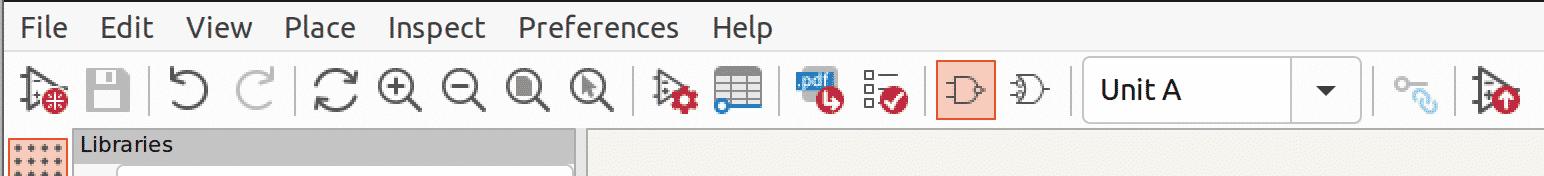
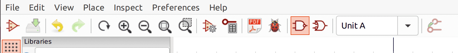
Toolbars have also been updated. Almost all buttons have been redesigned with an elegant modern look, but match one-on-one with their original counterparts from KiCad 5.
In Pcbnew you will find that the right toolbar has been greatly expanded to include many brand-new productivity-enhancing tools.
Most dialogue boxes have also been redesigned.
Both Eeschema and Pcbnew have updated Setup dialogue boxes under the File menu. With these dialogue boxes, you can define many of the attributes of your schematic and layout design working environments.
These Setup windows also existed in KiCad 5, but in KiCad 6 they were expanded to include features distributed in other menus and windows. Having one place with all (or at least most) configuration capabilities represents another productivity boost.
In Eeschema, the Electrical Rules Check capabilities are expanded. You now have more control over the customisation of the severity level of many violation types, and an updated pin conflicts map.
Similarly, in Pcbnew, you will find an expanded Design Rules control panel which includes a brand-new rules editor. With this editor, you can use S-Expressions to create custom design rules.
Cool fact: PCB fabricators will be able to create their KiCad DRC rules that you can import to your project and ensure compatibility of your design with their manufacturing capabilities.
KiCad 6 has a new theme color editor. You can now customise your KiCad work environment with your choice of colors. The colors of much of the user interface elements can be customised. Not only that, but you can define any number of theme presets, and enable them whenever you want.
Finally, KiCad 6 adds the ability to import PCB projects from CADSTAR. It also improves the import function for Autodesk’s Eagle. I have done some testing of the Eagle import function, and while it is better than before, there is still a lot of room for improvement.
Let’s continue with a deep dive into KiCad 6, starting with Eeschema, and continuing with Pcbnew.
Eeschema in KiCad 6
When you start Eeschema in KiCad 6, you will immediately see the familiar KiCad 5 organisation of the menus and toolbars, even with the new icon set for the buttons.

Kicad 6: Eeschema

Kicad 5: Eeschema
Let’s look at some of the most significant changes.
Schematic editing paradigm upgraded
A frequent complain voiced by KiCad users, old and new, is the way the the schematic editor reacts to user events. Prior to KiCad 6, Eeschema implemented an idiosyncratic editing paradigm that is unlike not just how things work in other CAD applications, but in other applications in general (word processing, email, etc).
Here's an example of how weird KiCad 5 (and older) can be. Open or create a new KiCad 5 project, open Eeschema, and click on any symbol. When you click on the symbol, information about it appears in the info bar at the bottom of the Eeschema window. It looks like this:

KiCad 5, Eeschema. When you click on a symbol, its information appears in the info bar.
Now, after you click on the symbol and its information appears in the status bar, move the cursor away from the symbol, and press the "E" key (which should bring up the symbol properties window). Normally, you would expect that because this symbol is the last thing that you clicked on, it would still be selected, waiting for your next action. You should be able to click on the "E" key and see the properties window.
Right?
Well, no. Eeschema in KiCad 5 and older doesn't work like that. When you click on a symbol or other item the only thing that happens is to show its information in the status bar.
The click does not select the item.
The position of the cursor selects the item.
This is totally weird, and I have seen first hand how this confused me, and my students. Even Pcbnew in KiCad 5 does not work like this. Pcbnew in KiCad 5 works as expected, where you click on an item and the item becomes selected so you can then perform actions like to move it or bring up its properties (try it!).
I am ecstatic to report that KiCad 6 Eeschema has finally changed its editing paradigm so that it works as expected.
In KiCad 6, when you click on an item in the schematic, the item is visible selected (you can see a blue outline around the resistor in my example below), and remains selected even as your mouse pointer moves elsewhere, and until you click on something else.

KiCad 6, Eeschema, I have clicked on an item to select it, and the item becomes highlighted.
With the item selected, you can use any of the available commands to do things such as move, drag, rotate, edit, copy, etc.
There are even some functions that will work with multiple selected items, such as move, drag, and copy.
Considering how much time people spent working on schematics, this new editing paradigm for Eeschema in KiCad will go a long way to reduce friction for new and current users alike.
My hope for a future enhancement: the ability to multiple select symbols of the same time and bulk assign a value. For example, select all LED current limiting resistors and set the same value in one or two clicks.
Back-import and footprint association file
Looking at the top toolbar I noticed that one missing button is the back-import.

KiCad 5, Eesceha, the back-import button.
This button facilitated the importation of changes from Pcbnew into Eeschema via the Symbol Footprint Link file (or "Footprint association (.cmp) file"). To make this work, you would have to first export this file from Pcbnew, and then import it into Eeschema.
This function is now handled by Update Schematic from PCB under the Tool menu.
In KiCad 6 Pcbnew, you can still export the Symbol Footprint Link file, except that it is now called "Footprint Association (.cmp) file" and is found under the File menu. Similarly, in KiCad 6 Eeschema, you can import a cmp file via the File menu.

KiCad 6, Pcbnew, Export a Footprint Assignments/associations file.

KiCad 6, Eeschema, import a Footprint Assignments/associations file.
One thing to note here is that terminology can still cause some confusion. The same file (cmp) is known as "Footprints Assignments file" (KiCad 6 and KiCad 5), "Footprints Associations File" (KiCad 6 and KiCad 5) or "Symbol Footprint Link File" (KiCad 5). In KiCad 6, the CMP file has one less name.
Schematic Setup
Under the File menu, you will now find a brand-new dialogue box: the Schematic Setup. You can also access the Schematic Setup dialogue via the top toolbar, where a new button appears right next to the save button.

Kicad 6: Eeschema, you can open the Schematic Setup dialog box from the File menu.

Kicad 6: Eeschema, you can open the Schematic Setup dialog box from the top tool bar.
You can access the Schematic Setup dialogue box via the File menu or the top toolbar.
The Schematic Setup dialogue box contains several new configuration options. It also hosts configuration options that existed in KiCad 5 but organised differently.
In KiCad 5, most settings were accessible via the Preferences dialogue box under the Preferences menu item. The same Preferences dialogue box is still available in Kicad 6.
Here are the items that stand out in the Schematic Setup dialogue box:

1. KiCad 6 - Formatting

2. KiCad 6 - Field Name Templates

3. KiCad 6 - Pin Conflicts Map

4. KiCad 6 - Violation Severity

5. KiCad 6 - Net Classes

6. KiCad 6 - Text Variables
General - Formatting
Under the General group, you will find the Formatting and Field Name Templates dialogues.
The Formatting dialogue allows you to set your preferred default text sizes, symbol line thickness, junction dot size etc. Most of these options are available in KiCad 5.
General - Field Name Templates
The Field Name Templates is a feature inherited from KiCad 5 verbatim, except that in KiCad 5 it appeared in the Preferences dialogue box.
Interestingly, in the nightly build version of KiCad 6 that I am testing at the moment (KiCad 5.99 of January 12, 2021), the Field Name Templates dialogue appears under both Schematic Setup and Preferences.
But, they are not the same! The difference between these two identically named field is the scope.
The Field name Templates in Schematic Setup have a project scope, whereas the one in the Preferences field has a global scope.
To test this feature, I have created a Field Name Template via the Schematic Setup dialogue box (which has project-level scope), and the Preferences (which has global scope).
These templates appear in the Symbol Properties field list, and in the Symbol Fields list, I can type custom text.
You can open the Symbol Properties dialogue by doing a right-click on a symbol and selecting “Edit”.
You can open the Symbol Fields dialogue box by clicking on the button that looks like a spreadsheet in the top toolbar.

My two custom field templates appear in the Symbol Properties fields list.

My two custom field templates appear in the Symbol Fields list.

Access via the spreadsheet button in the top toolbar.
Text substitution
Text Substitution is a brand-new feature to KiCad 6.
With text substitution, you can create a variable that contains arbitrary text and display this text anywhere in the schematic where text can appear.
The new text substitution feature is also available in Pcbnew.
Here’s a quick demonstration of how this works.
First, you can define your text variables in the Text Variables pane under the Project grouping of the Schematic Setup dialogue box.
You can see an example in my screenshot titled “6. KiCad 6 - Text Variables” (above).
Next, create something that contains text, such as a net label or a text item.
To display the value of the text variable, use the notation “${name_of_variable}”.
The result is that KiCad will replace all variable placeholders’ occurrences with the variable’s value, as defined in the Schematic Setup dialogue.
You can also use syntax conventions to control how the text looks. There is a handy Syntax Help window with more information.

This text item contains a text variable placeholder. In the schematic behind the Text properties dialogue, you can see the rendered variable.

You can control the text attributes through a specialised markup language. Syntax help is available via a hyperlink in the Text Properties dialogue.
Text substitution even works in the title block, in symbol properties and hierarchical sheet properties:

Set a text variable placeholder in Page Settings (under File).

KiCad 6 will render the variable in the title block.

Text substitution works in symbol properties. In this example I have parametrized the value of this resistor.
Here is an example of how text substitution works with sheets and sub-sheets. In the screenshots below, first I have created a sub-sheet with the name "Sample-subsheet". In the sheet properties, I have created a new field, with name "SubsheetResistorValue" (apologies for the boring names).
In the sub-sheet, I have created a resistor, and in its value property I have referenced the field "SubsheetResistorValue". KiCad will resolve the property reference with its set value.

KiCad 6, Eeschema: this sub-sheet contains a custom field.

KiCad 6, Eeschema: within the sub-sheet, I can use text substitution to resolve the value set for the sub sheet-level custom field.
Bye-bye netlist button
Before KiCad 5, the link between Eeschema and Pcbnew is the Netlist.
In KiCad 4, every single time that you made a change to the schematic, you had to create a new netlist file manually and (again, manually) import it into Pcbnew.
KiCad 5 provided a more seamless way of linking the two apps, but you could continue using the Netlist method as if you were using KiCad 4.

KiCad 5, Eeschema, Generate Netlist File via the Tools menu.

KiCad 5, Eeschema, Generate Netlist File via the top toolbar.
In KiCad 5, the Netlist button was still present in the top toolbar. My people used to it from the KiCad 4 years (myself included), continued to use it even though it was not necessary.
In KiCad 5, the correct way to import a schematic from Eeschema into Pcbnew was via the "Update PCB from Schematic" button. This method is also available in KiCad 6, and it remains the proper way of importing a schematic into Pcbnew.
In KiCad 6, the Netlist button has been removed from the top toolbar.
You will find the Netlist export and import functions under the File menu in Eeschema and Pcbnew respectively.

KiCad 6, Eeschema: Netlist Export is hidden in the File menu.

KiCad 6, Pcbnew: Netlist Import is hidden in the File menu.
In KiCad 6, the netlist button is missing in an effort to simplyfy the workflow. You can import schematic data (and updates from already imported data) to Pcbnew by clicking on the new “Update PCB with changes made to schematic” (found in the top toolbar in Pcbnew).

Kicad 6, Eeschema: no netlist file needed.

Kicad 6, Pcbnew: no netlist file needed.
Let's recap.
In KiCad 6, you can update Eeschema with changes in Pcbnew and vice-versa with these two commands:
Both are available under the Tool menu in either app.
Interactive delete tool
A new tool that is designed to make it easier to edit complicated schematics is Interactive Delete.
You will find it under the Edit menu (but I think it is useful enough to eventually have its own keyboard shortcut and button in the top toolbar).

KiCad 6, Eeschema, the Interactive Delete Tool.

I have enabled the Interactive Delete Tool. The symbol for R6 is highlighted and is deleted once I click.
Once you select the Interactive Delete Tool, the mouse pointer changes to an eraser. As you hover the pointer over a schematic item (such as a symbol, wire, text label etc.), that item is highlighted.
This way you can be sure that the item you are about to delete is the correct one. Just click to delete the highlighted item. This is a new productivity feature that will reduce the dreaded “Doh!” moments to a minimum.
Edit text and graphics
KiCad 6 gives you the ability to customise almost every aspect of the way that schematic items look like. Colours, line widths, orientation, and decorations are all configurable.
Under the Edit menu, you will find the new “Edit text and graphics” tool which allows you to edit such attributes in bulk.
The tool allows you to do this in two steps:
-
1Select the type of items you want to change their appearance using a scope selector or a filter.
-
2Define new visual attributes (such as text size, orientation, and alignment).

KiCad 6, Eeschema: the Edit Text and Graphics Properties pane.

I have changed the size and alignment of all wire labels with a couple of clicks.
As with the Interactive Delete Tool, the Edit Text and Graphics tool is another example of how KiCad’s development focuses on providing ways to make us more productive.
Change symbol
Another new tool that I’ve been hoping for is the Change Symbols tool. You’ll find it under the Edit menu.
This tool allows you to change the symbol used for multiple schematic objects at once.
Similarly to the Edit Text and Graphics Properties tool, the Change Symbols tool provides a way to select a specific class of items. Items can be matched by reference designator (for example “R?” will match all items with a designator that begins with “R”), a value, and a library identifier.
Once you have selected the class of items you want to change their symbol, you can specify the new symbol identifier.
In the example below, I am changing the symbol of all resistors (using the “R?” expression) to the resistor’s US symbol.

KiCad 6, Eeschema: The three resistors are using the EU symbol. Let’s change them to the US symbol using the Change Symbols tool.

I have matched all symbols with a designator that begin with “R” and changed their symbol to Device:R_US.
Context menu
The context menu in KiCad 6 Eeschema is more powerful then ever before. Multiple new functions are available with the click of a button. Several of them are available in KiCad 5, but were accessible elsewhere and with more than one click, or through a shortcut (such as the Rotate function).
For example, in KiCad 5, to edit the value of a symbol you would need to drill into the Properties submenu. In KiCad 6, you can click on the Edit Value function at the root context menu.
In KiCad 5, the Rotate function is also available via a shortcut or through the Orientation submenu. In KiCad 6 it is available at the root of the content menu (all shortcuts work as expected). Most items in the KiCad 5 Properties and Orientation submenus like in the root context menu of KiCad 6 Eeschema.
The Open Documentation function (KiCad 5) is changed to Show Datasheet (KiCad 6).
Here are the KiCad 6 and KiCad 5 versions of the context menu in Eeschema, as it applies on a symbol:

KiCad 6, Eeschema, context menu for a symbol.

KiCad 5, Eeschema, Context Menu for a symbol.
Functions like Move and Drag remain. New ones are added:
- Align Elements to Grid.
- DeMorgan Conversion.
- Change and Update Symbol.
- Show Datasheet.
- Edit Page Number.
- Select All.
Finally, in KiCad 5 Eeschema context menu, the last function is "Close". I never understood the purpose of this function, since to close the context menu you simply click outside the menu. In KiCad 6, the "Close" function is removed.
Enhanced bus handling
In KiCad 6, signal bus handling is vastly improved. Both the user interface used to draw and wire busses, as well as the underlying infrstructure of naming the nets and groups of nets that belong to a bus, are all improved.
Let's begin with the UI. In the screenshot below, I have drawn a bus line. The, I have called the Line Style dialogue box (you can double click on the bus, type "E" as the mouse pointer is over the bus, or use the context menu and select "Properties"). It looks like this:

KiCad 6, Eeschema, bus line properties.

KiCad 6, Eeschema, bus line style options.
The ability to configure the visual aspects of a bus means easier to read schematics. For example, you can set your data bus to be red, and your address buss to be blue. In KiCad 5, busses did not have properties at all.
While the ability to visually customise a bus is useful, it represents only a small set of upgrade in the way that busses work in KiCad 6. The bulk of the new features is in the way that nets can be bundled in a bus.
In KiCad 5, it is possible to create a bus that can "carry" signals that are labeled according to a simple convention. Here is an example:

KiCad 5, an example of a bus.
In the example above, I show a typical way in which a bus is used in KiCad. There are many more. In the example, I have a connector on the left side with 4 pins. I have used local labels to name the nets that are connected to the pins. The labels are:
- DATAOUT0
- DATAOUT1
- DATAOUT2
- DATAOUT3
I have given membership of those nets to the bus by using the label construct "DATOUT[0..3]". An alternative way would be to use bus entry wires for each of the nets.
On the right side of the example I have placed a second connector. I have labeled the nets that connect to the left connector pins like this:
- DATAIN0
- DATAIN1
- DATAIN2
- DATAIN3
Just like with the left connector, I have used the label construct "DATIN[0..3]" to give the DATAINx nets membership to the same bus.
KiCad is smart enough to work out the relations between the nets:
- DATAOUT0 connects to DATAIN0
- DATAOUT1 connects to DATAIN1
- DATAOUT2 connects to DATAIN2
- DATAOUT3 connects to DATAIN3
This is a classic example of when you would use a bus, instead of simply relying on net labels.
In KiCad 6, the bus label notation for net membership is far more powerful. You can now use a wide range of label constructs. You can see the valid syntax below:

KiCad 6, Eeschema, bus definition syntax.
You can find the Syntax Help window by double-clicking on a bus and then click on the Syntax Help hyperlink.
In the list of Bus definitions from the Syntax Help window, the first two are inherited from KiCad 5, and the rest are brand new. All of the new bus definitions use curly brackets, similar to how we can now define text variables.
Let's look at some of them (drawing from the syntax help examples):
- Mix nets of arbitrary names. For example: {dat1 dat2} would create nets dat1 and dat2 inside the bus.
- Nets that don't have a numerical suffix, such as {SCL SDA} or {DP DM}.
- You can have named buses by adding the name on the left side of the opening curly bracket: USB1{DP DM} would create nets USB1.DP and USB1.DM.
- Mix nets with different prefixes, and even combine pre-KiCad 6 bus definitions with new definitions : {D[0..7] LATCH} would create nets D0, D1, ..., D7 and LATCH.
- You can even use markup symbols, such as "~" for overbar and "_" for subscript.
With all these convenient ways to add nets to a bus, you may be wondering how to extract individual wires for each embedded net so that you may connect to to other parts of the schematic graphically, as opposed to using the net labels.
Let me show you a neat new trick.
Here's a bus, with a fairly elaborate net definition:

KiCad 6, a bus with a convoluted net definition.
The bus definition creates a total of 6 nets. To extract individual net wires from the bus, you can use the new "Unfold from Bus" context menu option, drill down to the net that you want to extract, and then draw it as you wish. It looks like this:

KiCad 6, right click on a bus to inspect the nets it contains, and create a wire for each one.

KiCad 6, a bus with two of its nets unfolded.
As you can see, it is not easy from create buses that bundle together a large number of nets, and just as easy to unfold them graphically. As a consequence, the bus definitions can become long and convoluted. Display the entire definitions in the label attached to a bus may make the schematic look too busy.
In KiCad 6, there is a new way to deal with this complexity. Under the Tools menu, you will find a new option: "Bus Definitions". This will bring up a dialog box in which you can create a bus alias that may contain one ore more alias members. An alias member is a simple of complex net definition.
See my example below, in which I have replaced the complex bus definition from my previous example with a single bus alias named "MEM" that contains two simpler bus definitions. The end result is the same, electrically speaking, but the schematic is easier to read.

KiCad 6 has a new Bus Definitions dialog box.

The Bus Definitions allows to you create bus aliases that contain one ore more net alias members.

Bus aliases and all their member nets can be attached to a bus by referencing the bus alias name.
To attach a bus alias to a bus, simply create a label with the name of the bus alias in between curly brackets. The member nets are now part of the bus, and they can be unfolded via the context menu.
Jon Evans has created a short video where he demonstrates the new bus features in KiCad 6. Check it out: Jon Evan's bus upgrades demo.
Pcbnew in KiCad 6
Many of the changes found in Eeschema are also found in Pcbnew. For example, there is a brand-new Board Setup dialogue box which is the equivalent of the Schematic Setup dialogue found in Eeschema.
Also, Pcbnew in Kicad 6 contains many improvements in the layout drawing capabilities and brand new productivity and convenience features.
Let’s dive in for a closer look.
(New) right toolset
The most significant visual change in Pcbnew of KiCad 6 is the redesigned right-side toolset.
This toolset contains an updated toolbar and three new groups of widgets: Appearance, Presets, and the Selection Filter.
In the screenshots below you can see a side-by-side comparison between the KiCad 6 (left) and KiCad 5 (right) right toolset in Pcbnew. I have marked the elements of the KiCad 6 Pcbnew right toolset with their names. I will refer to these names in the discussion that follows.

The right toolset in KiCad 6 Pcbnew.

The right toolset in KiCad 5 Pcbnew.
In KiCad 5, the Pcbnew right toolset consisted of a toolbar with various drawing tools and the Layers Manager. The Layers Manager contained two tabs: Layers, useful for selecting the active layer on which editing took place, and Items, useful for hiding and showing layout times.
In KiCad 6, the right toolset is turbo-charged.
It retains the vertical toolbar, updated with new icons and a few multi-tool buttons (more about this later).
It also retains the Layers tab in the renamed Appearance box. The Appearance box takes up most of the real estate of the right toolset, and it also contains the Object tab (which inherits the functionalities of the old Items tab and adds a few new ones), and the new Nets tab.
The Nets tab provides widgets that allow you to control the visibility of individual Nets or Net Classes.
Appearance: Layers
In KiCad 6, the Layers tab works similarly to its namesake in KiCad 5, but it is much improved.
When you select a layer to activate it, this layer’s elements will come to the foreground, and everything else will recede in the background. This makes it much easier to identify elements in a busy circuit.
The foreground/background visual effect is enhanced significantly using the Layer Display Options group’s radio buttons.
See this example:

I have selected the back copper layer (“B.Cu”) from the Layers tab and checked the Dim option from the Layer Display Options group. You can see the effect of this. The blue tracks that belong to the back copper layer stand out, while everything else is dimmed. Even with the busiest of circuits, you will not have much trouble identifying the elements that belong to the currently active layer.
Appearance: Objects
The Objects tab allows you to control the visual aspects of layout objects such as tracks, footprints and ratsnests.
You can control the opacity of tracks, vias, pads and zones, as well as the visibility and colour of 15 other objects.
Here’s an example:

KiCad 6, Pcbnew, pads are dimmed.

KiCad 6, Pcbnew, pad opacity is maxed-out.
In this example, I manipulate the opacity of the pads. In the left screenshot, I decrease opacity, while in the right I have increased it. In both screenshots, you can also see a net depicted with a custom green thin line.
Appearance: Nets
The Nets tab allows you to control the colour of nets and ratnests.
Again, I’ll explain how this works with an example.
See the screenshot below:

The arrows show the points of interest.
You can show or hide each net and set its colour individually. In this example, I have set the colour for the GPIO39 net to green, and D1-Pad2 net to red. In the Net Colors radio buttons under the Net Display Options group, I have selected “All”.
The effect of this is that the colour that I have assigned to these nets is applied to both ratnests, tracks, and pads that belong to these nets.
With the tracks, the custom net colour (red) and the net display options are overriding the default layer colour. This way it is possible, for example, to assign a colour to significant nets, such as the Ground net, so that I can see all traces that belong to this net regardless of which layer they are on.
That’s neat.
Presets
The Layers, Objects and Nets tabs contain lots of widgets that allow you to fine-tune how your PCB layout is displayed.
Eventually, you will find your self working with a regular set of configurations.
This is where the Presets drop-down comes in handy.
With a single click, you can assign your desired setting to the widgets of all three tabs. There are several defaults presets to choose from, but you can also save your custom settings.
Here’s the expanded Presets menu, showing the default presets:

Here’s how powerful Presets is. In the screenshot of the left side (below), all layers and objects are enabled. In the left screenshot, I have selected the “All Copper Layers” preset. This preset makes everything disappear except for the objects in the front and back copper layer (tracks, pads, zones, and vias).


Clarity with a single click.
Selection Filter
The last new addition to the right toolset in KiCad 6 Pcbnew is the Selection Filter.
In my time playing with KiCad 6, this is probably the productivity tool I use most often.
The Selection Filter allows you to control which type of object will respond to your mouse clicks or group selections.
Let’s look at an example of. See the two screenshots below.


In the left screenshot, I have enabled all objects. When I do a right-click on an area where a footprint and a track overlap, Pcbnew will ask me to choose which object I want to select.
In the right screenshot, I have selected on “Tracks” in the Selection Filter. When I right-click on the same area as in the left screenshot, Pcbnew will immediately display the context menu for the track, since it “knows” that I am only interested in tracks.
The Selection Filter also works with multiple selections. See below:


With only Tracks selected from the Selection Filter options, I click and drag to select several tracks (left screenshot). When I release the mouse, the selected track segments remain highlighted. Pcbnew did not ask me for clarification, nor did I have to worry about accidentally moving footprints or other elements.
Vertical toolbar: multitools
The last component of the right toolset that I will describe in this article is the vertical toolbar.
It contains all of the buttons found in the right toolbar from Pcbnew in KiCad 5, with a few additions.
You can see them here, side by side:

KiCad 6, Pcbnew, right toolbar.

KiCad 5, Pcbnew, right toolbar.
The icons are updated, and modern-looking, with several multi-tool buttons and one new function added.
The multi-tools allow you to access functions that were previously accessible via the menus. Here’s a list:
-
1Single track and differential pairs router. You can see this multi-tool opened in the left screenshot above.
-
2Microwave applications track tool, for creating tracks and stabs of specific lengths, specific gaps, as well as arcs and polygons.
-
3Measurements tool, for adding linear, orthogonal, centre and leader dimensions.
-
4Origin points tool, for setting the grid origin point and placing the origin point for drill files and footprint position files.
You can see these multi-tools below:

1. Track tool.

2. Microwave applications track tool.

3. Measurements tool.

4. Origin points tool.
Vertical toolbar: Rule areas
The vertical toolbar in KiCad 6 Pcbnew contains a brand-new button: the Rule Area tool.

KiCad 6, Pcbnew: the new Rule Area button.

KiCad 6, Pcbnew, Rule Area properties.
With the Rule Area tool you can create arbitrary keep out areas. You can set the properties of the Rule area to keep out tracks, vias, pads, copper pours or footprints. You can also restrict the application of the rule area to specific copper layers, and give it a name.
The name will help you identify violations in the DRC report.
In the screenshots below I show a small keep-out zone.

Keep out zone prevents tracks from being drawn inside the zone.

The DRC generates an error if it detects a footprint inside the keep-out zone.
First, I try to draw a track inside it (see left screenshot). The push & shove router will correctly prevent me from doing so. Notice that my mouse pointer is well within the keep-out zone, but the track is only drawn up to the edge of the zone.
Second, I place a mounting hole footprint inside the keep-out zone. I did not get a warning in real-time, but when I ran the Design Rules Check, a violation was produced:

Board setup
Pcbnew now has a comprehensive Board Setup dialogue box. You can access it from the File menu and via a button in the top toolbar.
Unlike with the Schematic Setup in Eeschame, the Board Setup in Pcbnew is not new. It was present in KiCad 5. However, in KiCad 6, Board Setup is significantly expanded to contain many new configuration options and provide a new “home” for configuration dialogues that were organised differently in KiCad 5.
For example (see screenshots below), in KiCad 5, the Board Setup dialogue contains the Text & Graphics pane in the Layers group. It allows you to set visual default properties for items such as lines and text. In KiCad 6, the same pane is titled “Defaults” and contains additional configuration options.
As is evident from the screenshots below, the new Board Setup dialogue contains many more configuration options than it did in KiCad 5.

KiCad 6, Pcbnew, the Board Setup dialogue box.

KiCad 5, Pcbnew, the Board Setup dialogue box.
Let’s look at these options as they are grouped.
Board Stackup
The items in the Board Stackup group are not new.
The KiCad 6 “Board Editor Layers” pane is accessible by clicking on the “Layers” group header in KiCad 5.
As you can see in the screenshots below, the two panes are almost identical.
However, one difference stands out: In KiCad 6, you can add custom layers by clicking on the “Add User Defined Layer”.

KiCad 6, Board Setup, Board Editor Layers.

KiCad 5, Board Setup, Layers.
The new Board Stackup group contains two brand-new panes: Physical Stackup and Solder Maker/Paste (see below):

KiCad 6, Board Setup, Physical Stackup.

KiCad 6, Board Setup, Solder Mask/Paste.
In Physical Stackup, you can set the board’s thickness and the individual characteristics of each board layer, including the type of material used, its thickness, and the colour to depict it in the editor.
In Solder Mask/Paste, you can set attributes such as the solder mask clearance and its minimum bridge width. These are numbers that you can obtain from your preferred PCB manufacturer and help ensure that your PCB design will be manufacturable.
Text & Graphics
In the Text & Graphics group, you will find the Defaults and the Text Variables panes.
The former also existed in KiCad 5 but under a different name. It was “Text & Graphics” in the Layers group:

KiCad 6, Pcbnew, Board Setup, Text & Graphics Defaults.

KiCad 5, Pcbnew, Board Setup, Text & Graphics.
The two panes share the same fundamentals, but in KiCad 6, there are additional configuration options.
The Text Variables pane is new and performs the same function as its counterpart in Eeschema (which I described earlier under “Text Substitution”).
You can see an example of how Text Variables work below:

KiCad 6, Pcbnew, Text Variables, I have created a new text variable with an arbitrary text value.

The text label contains a reference to the text variable. KiCad will replace the reference with the actual value.
Text variables work with anything that contains text, such as text items, and labels.
Design Rules
The Design Rules group is a “mixed bag” concerning new and updated configuration options.
The Net Classes pane is inherited from KiCad 5 unchanged.
The Solder Mask/Paste pane, which was under Design Rules in KiCad 5, has been moved to the Board Stackup group in KiCad 6. Apart from the move to a new group, this pane is also unchanged.
The Pre-defined Sizes pane allows you to creates any number of predefined sizes for tracks, vias and differential pairs. In KiCad 5, this pane was titled “Track & Vias”. Apart from the name change, everything else remains the same.
KiCad 6, Pcbnew, Board Setup, Design Rules, Net Classes.

KiCad 6, Pcbnew, Board Setup, Solder Mask/Paste.

KiCad 6, Pcbnew, Board Setup, Design Rules, Pre-defined Sizes.
The rest of the panes in this group are new:

KiCad 6, Pcbnew, Board Setup, Design Rules, Constraints.

KiCad 6, Pcbnew, Board Setup, Design Rules, Custom Rules.

KiCad 6, Pcbnew, Board Setup, Design Rules, Violation Severity.
Fillet tracks
In KiCad 6, you can create tracks with rounded corners. This function is titled “Fillet tracks” and is available through the context menu by right-clicking on a track.
The process begins with a single or multiple tracks as you can apply fillet tracks on multiple tracks simultaneously through multiple-selection.
Select the segments of a track (or tracks) that contain the angles that you want to fillet, and click on the right mouse button to reveal the context menu.
Select the Fillet Tracks option. In the popup that appears, set the radius of the fillet in millimetres. Values larger than 1mm produce curvier angles.
Click on OK, and you will see that the original 90-degree angle becomes a more natural-looking curve.

KiCad 6, Pcbnew, Fillet track, Step 1: Start by selecting the two segments of a track that contain an angle.

KiCad 6, Pcbnew, Fillet track, Step 2: Right-click on the selected track to reveal the context menu. Click on Fillet Tracks.

KiCad 6, Pcbnew, Fillet track, Step 3: Set the fillet radius in mm.

KiCad 6, Pcbnew, Fillet track, Step 4: Marvel on the curved angle.
In my testing, I found that the fillet function only works with 90-degree angles. If you have tracks that contain 45-degree angles, you will not be able to convert them to curves.
You can also select multiple 90-degree tracks and fillet them at the same time. Here is an example:

You can fillet multiple tracks that contain 90-degree angles.

The result is a more natural and organic looking PCB.
Filled zones
In KiCad 6, filled zones have received two notable upgrades:
-
1Hatched fill.
-
2Zone names.
In KiCad 5, the only possible fill for filled zones was solid. Solid fills provide are simple and provide good resistive characteristics. But when used with thinner substrates, they can cause warping and even form bubbles under the copper.
To prevent such defects, you can use hatched fill for the copper zones. This is now possible in KiCad 6.
Here’s a comparison of the fill zone configuration dialogue boxes. KiCad 6 is on the left, and KiCad 5 on the right.

KiCad 6, Pcbnew, Filled Zones configuration.

KiCad 5, Pcbnew, Filled Zones configuration.
The is a new group of widgets titled “Fill” in the right side of the KiCad 6 Copper Zone Properties window. The Fill Type drop-down allows you to select “Hatch pattern”, and select the various attributes for this fill. I have set 0.5mm for hatch width and gap.
The result of this configuration is below (showing a segment of the fill, compared to the solid fill from KiCad 5):

KiCad 6, Pcbnew, hatch fill example.

KiCad 5, Pcbnew, solid fill example.
A second new feature concerning Copper Zone in KiCad 6 is that zone can now have names. You can see the Zone name text field in the widgets General group (see screenshot below).

KiCad 6, Pcbnew, Filled Zones name.
Curved ratsnests
KiCad 6 introduces curved ratsnest lines! This may not seem like a big deal, but check this out:

KiCad 6, Pcbnew, curved ratsnest lines.

KiCad 5, Pcbnew, straight ratsnest lines.
Along with the ability to customise the colour of the nets, the curved ratsnest lines on the left (KiCad 6) look much better than those on the right (KiCad 5).
Of course, curved vs straight lines is a personal choice, and KiCad 6 does not take this away from you. You can access this option from the View menu. Here’s a side-by-side comparison:

KiCad 6, Pcbnew, straight ratsnest line.

KiCad 6, Pcbnew, curved ratsnest line.
Interactive router
The interactive router in KiCad 6 has also received a lot of attention. There are several new configuration options available in the Interactive Router Setting dialogue box (see below, KiCad 6 on the left, KiCad 5 on the right).
The new options are:
-
1Optimise track being dragged.
-
2Use mouse path to set track posture.
-
3Fix all segments on click.
In my limited testing, I found that the interactive router worked perfectly. My PCBs are relatively simple, and even in KiCad 5, I did not encounter any issues worth mentioning here.

KiCad 6, Pcbnew, Interactive Router Settings.

KiCad 5, Pcbnew, Interactive Router Settings.
Updated coordinate system
In Pcbnew, the coordinate system has been a source of frustration, especially for people moving in after using other tools.
I was fortunate enough to start using KiCad after more than 15 years of not having used any other CAD application. During this time, I totally forgot any non-KiCad conventions, so everything in KiCad felt normal, including its coordinate system.
But the KiCad developer team recognises that KiCad is not the only "game" in town. For KiCad to increase its share, it must play better with widely accepted norms and standards. One of those norms is the way that the coordinate system works in Pcbnew.
The coordinate system is a fundamental concept in any drawing application. Pcbnew is, essentially, a drawing application for printed circuit boards. Its coordinate system assumes that the (0,0) coordinate starts at the top left corner of the page (see annotated screenshot below). You can adjust the origin left or right. And that's about it.
But, most (maybe all?) other drawing, mechanical or PCB programs assume that the origin is at the bottom left of a page.
This discrepancy between KiCad and everyone else causes several problems.
First, users coming to KiCad from other tools have to adjust working with the new coordinate system. After years of a bottom-left coordinate system, getting used to top right is easier said then done (example: I still used Netlists in KiCad 5 because muscle memory is hard to forget).
Second, interoperability with other drawing tools is much harder when coordinate systems don't agree. At the very least, it will cost you a bit of time to translate X and Y numbers. At the worst, you could crash your robotic probe to Mars (doh!).

In KiCad, the default coordinate system starts at the top left of the page.

Everyone else (?) coordinate system starts at bottom left.
Here's the difference between KiCad 6 and KiCad 5 handling of the coordinate system configuration:

KiCad 6, Pcbnew Origin and Axes: now allows for Y to increase up.

In KiCad 5 and earlier there is no way for Y to increase up.
To set the KiCad 6 Pcbnew coordinate system so that the origin is at the bottom left (which ever point you choose), and for the Y coordinate to increase upwards, follow this process:
- Go to Preferences --> Preferences, and select the Origins & Axes pane.
- Select these options (also see screenshot above):
- Display Origin --> Grid origin
- X Axis --> Increases right
- Y Axis --> Increases up
- Display Origin --> Grid origin
- Select the "Set grid origin point" tool from the left tool bar (see screenshot below).
- Click at the location where you want to set the origin.
- That's it.

This tool allows you to set a custom grid origin point.

The grid origin symbol marks the spot.
Once you have set the new origin point, and the Y coordinate to increase up while the X coordinate increases right, you have a coordinate system that is compatible with most (all?) drawing programs. In the screenshot below you can see that the location of the cursor is reported based on my custom coordinate system rather than KiCad's default.

My KiCad now has a coordinate system that is compatible with that of other drawing programs.
Create nets in Pcbnew
It is easy to create and use nets in Pcbnew. There's a few ways you can go about doing that.
For example, you can create a new net via the Net Inspector dialogue box (in the "inspect" menu). Once you have a net, you can assign a track to it through the track's (or pin's) properties.

KiCad 6, Pcbnew, you can create a new net via the Net Inspector dialogue box.

KiCad 6, Pcbnew, assign a net to a track.
It is also possible to create and assign a net in a single step. See example below. I have drawn a track, and brought up its properties. In the Net drop-down, I type the name of the net I want to create. If the name does not already exist, KiCad will offer to create it, and then assign it to the track.

KiCad 6, Pcbnew, create and assign a net in a single step.
Board statistics
The Inspect menu contains another useful tool, Board Statistics. It does what the name suggests. The Board Statistics dialogue box will display general information about your board, such as its components, pads, vias, and size, as well as drill hole sizes and locations.

KiCad 6, Pcbnew, Show Board Statistics.

KiCad 6, Pcbnew, general board statistics.

KiCad 6, Pcbnew, drill statistics.
You can also export these statistics in a text file:

KiCad 6, Pcbnew, statistics exported TXT file.
Infobar
I have not had the opportunity to explore this feature much, but it did draw my attention a couple of time.
Its a new, less obstrusive, way for KiCad to communicate with you: the Infobar.
For events that are not important enough to disrupt your workflow, but sufficiently important to warrant a notification, KiCad 6 uses a narrow bar just below the top tool bar. See below:

KiCad 6, Pcbnew, the infobar is a way for KiCad to communicate with you without breaking your workflow.

KiCad 6, Pcbnew, inforbar example.
I did not have much opportunity to see the infobar in action because during my testing I did not trigger it enough. In the example above (left), I managed to trigger it by editing the footprint of a hole. The infobar informed me that I am editing the footprint that exists inside the board file, not the library. Therefore, any changes to this footprint will only apply to the board.
Good to know, but not earth-shattering, hence the infobar is a good way to handle this information.
Locking
In KiCad 6 Pcbnew, everything can be locked. Footprints, tracks, zones, text items, etc. In KiCad 5, on the other hand, only few items were lockable. Zones, for example, were not. Neither were text items, or graphics.
To lock an item, as was the case in KiCad 5, you can use the context menu or the item properties dialogue box.
Below, I show how a zone is lockable under KiCad 6 (left) but unlockable under KiCad 5 (right):

KiCad 6, Pcbnew, Zones are lockable.

KiCad 5, Pcbnew, zones are not lockable.
Here's two more examples. Left, showing a text items, which is lockable in KiCad 6 (not lockable in KiCad 5), and an alternateive way to lock an item via its properties dialogue box.

KiCad 6, Pcbew, text items are lockable.

KiCad 6, Pcbnew, you can lock an item via its properties dialogue box.
Groups
In KiCad 6 Pcbnew, it is possible to group any two or more items. Once you have a group, you can move it to a new location. All of the items in the group will move together in the new location.
To select a group, just click on any of the group's items.
The ability to group items together was not available prior to KiCad 6.

KiCad 6, Pcbnew, you can now create groups of any two items.

KiCad 6, Pcbnew, when you move a group, all the items within it will move along.
When you are finished working with a group, you can ungroup the enclosed items by selecting Grouping --> Ungroup from the contextual menu.
Draw a rectangle
- Line.
- Circle.
- Arc.
- Circle.
- Polygon.
KiCad 6 adds one more:
- Rectangle.
You can draw a rectangle by selecting the tool by that name from the right toobar. Then click where you want to draw the first edge of the rectangle, and click again where you want to draw the last edge. KiCad will finish drawing.
The process looks like this:

KiCad 6, Pcbnew, select the Rectangle tool and click to start drawing.

KiCad 6, Pcbnew, click again to finish drawing.
Context menu
In KiCad 6 Pcbnew, the context menu contains functions that can be applied immediately on the selected item. Most of these functions are carried over from the KiCad 5 Pcbnew context menu, but there are a few new items, plus some re-organisation.

KiCad 6, Pcbnew, example context menu (pad).

KiCad 5, Pcbnew, example context menu (pad).
At the top of the KiCad 6 Pcbnew context menu is the Select item, which contains a few sub-functions including the selection filter (that is also accessible via the Appearance pane in the right toolset). It is interesting to note that the Select item is present in KiCad 5, but is found towards the middle of the context menu.
Several of the movement function have been moved into sub-menus (such as the Special Tools for functions such as "Move Exactly" and "Move with Reference").
At the time I am writing this, there are a few new items in the Pcbnew context menu in KiCad 6:
- Grouping
- Select All
- Net Tools
- Copy Pad Properties to Default
- Paste Default Pad Properties to Selected
- Push Pad Properties to Other Pads...
The last three tools allow you to quickly propagate pad properties across your PCB. This was not possible prior to KiCad 6, and you would need to manually reset pad properties if you needed to make changes.
3D viewer and models
In KiCad 6, tthe 3D viewer has received a lot of attention. Not that the one in KiCad 5 was not up to the task, but in KiCad 6 there's are several new options to configure your PCB creation in 3D. Raytracing was available in KiCad 5 and has been brought over to KiCad 6, but is much more impresive (see below).
Let's start with a side-by-side comparison. KiCad 6 on the left, and KiCad 5 on the right.

KiCad 6, 3D viewer using default settings.

KiCad 5, 3D viewer using default settings.
First, click on the images above to see their full-resolution version.
The KiCad 6 version seems a bit more refined, but using the default settings both renders look great.
Here's the same view with raytracing turned on:

KiCad 6, 3D Viewer with raytracing on.

KiCad 5, 3D Viewer with raytracing on.
In the KiCad 6 version, notice that the LED are reflecting some of the sorrounding silkscreen. Very impressive!
As with KiCad 5, raytracing is heavy on resources. It is something you will keep turned off and only use it when you want to take a glamour shot of your PCB. But in KiCad 6, you have several options to speed up raytracing that are not available in KiCad 5.
Here's the raytracing display options for KiCad 6 (not available in KiCad 5):

KiCad 6, 3D viewer, raytrace viewer options.

KiCad 6, 3D Viewer, Raytracing lights configuration.
Reducing sampling or turning off options has a significant effect on the rendering time of new frames.
Next, I'll compare the other display options availabe in KiCad 6, and compare with KiCad 5 (you have alread seen the Raytracing options).
Below, the first two screenshots are from KiCad 6, and the last one from KiCad 5.

KiCad 6, 3D Viewer Display Options

KiCad 6, 3D Viewer, OpenGL options.

KiCad 5, 3D Viewer, options.
Here's some of the changes I have noticed:
- The Render Options group contains new options.
- The 3D Model Visibility, User Layers and Board Layers groups are unchanged.
- There's a new group that provides camera controls, such as the animation speed and the rotation increment.
- The OpenGL tab is new and allow you to balance the rendering quality against the framerate. Essentially, this is also the purpose of the Raytracing tab.
In terms of the 3D model assigned to the footprints, I did not notice much change. You can still assign a model to a footprint via the footprint's "3D Models" properties tab.

KiCad 6, 3D model to footprint assignment.

KiCad 5, 3D model to footprint assignment.
At the bottom left of the KiCad 6 Footprint Properties dialog box, notice a widget that allows you to set the model opacity. This is how you can make a model such as an LED seem semi-transparent. I can imagine applications of this feature in various kinds of displays, and perhaps PCB substrates.
In terms of the types of model files that KiCad 6 can read, clues are available in the 3D model chooser dialog box. You can open the chooser by clicking on the folder icon in the 3D Settings tab of the footprint properties dialog box (you can see this in the screenshots above).
First, here's the KiCad 6 and KiCad 5 versions of the model chooser dialog box:

KiCad 6, Pcbnew, footprint properties 3d model chooser.

KiCad 5, Pcbnew, footprint properties 3d model chooser.
In both cases, I have clicked on the dropped down widget below the file browser to reveal the supported files. From this comparison, you can see that Kicad 6 can read a large number of 3D model file formats, including IDF, EMN, WRL, X3D, etc.
Below is another screenshot that show the complete list (click to see full resolution version of the image):
KiCad 6, the supported 3D model file formats.
The list contains:
- IDF
- EMN
- WRL
- WRZ
- X3D
- STP
- STPZ
- STEP
- STP.GZ
- IGS
- IGES
Other improvements
In this section I discuss improvements that are introduced in Pcbnew and Eeschema.
Copy/paste
Copy/paste has had a difficult history in KiCad.
In KiCad 5, for example, Eeschema does not even have a copy function. It has "duplicate" instead. Pcbnew does have "copy", but you can only paste in the same Pcbnew instance. This situation is similar to not be able to copy text between two text editors.
This is less then ideal
In KiCad 6, copy and paste works across Pcbnew and Eeschema instances. For example, you can copy a footprint from a project instance of Pcbnew and paste it to a standalone insteance of Pcbnew.
You can do the same thing with Eeschema.
Here's a couple of examples. First, Eeschema.
In the next three screenshots, I show the copy and paste steps across two Eeschema instances.

KiCad 6, Eeschema, copy several elements to the clipboard.

KiCad 6, Eeschema, paste from clipboard.

KiCad 6, Eeschema, it is possible to copy items between separate instances.
Here is a similar example that shows how copy/paste works across separate instances of Pcbnew:

KiCad 6, Pcbnew, copy several elements to the clipboard.

KiCad 6, Pcbnew, paste from clipboard.

KiCad 6, Pcbnew, it is possible to copy items between separate instances.
Symbol Editor in KiCad 6
The Symbol Editor in KiCad 6 has also received an overhaul. You will find much of the new functionality of the KiCad 6 Eeschema app in the Symbol Editor.
Here's what the Symbol Editor looks like in KiCad 6, compared to KiCad 5:

KiCad 6, the Symbol Editor, editing a legacy symbol.

KiCad 5, the Symbol Editor.
New Symbol format
In the screenshots above, I am editing the same symbol to make comparison easier. At first, not much looks different. But a clue as to an important background change is in the infobox in the KiCad 6 Symbol Editor.
Take a closer look:

KiCad 6, Symbo Editor. Legacy symbols are read only until you migrate them to the KiCad 6 format.
In KiCad 6, Symbols and footprints utilize a new format, which is not compatible with the old format. KiCad 6 is able to import and migrate old symbols and footprints so that your existing (as well as legacy public domain) libraries will continue to work.
You can still incorporate symbols and footprints from old libraries into your projects, but you will not be able to edit them without migrating them.
You can easily migrate an old library with all its symbols via the Symbol Library Manager. You can invoke the manager through the Preferences menu item.
It looks like this:

KiCad 6, Symbol Editor allows you to migrate a library to the new format.

KiCad 6, Once you migrate a library to the new format, KiCad will remove the entry to the legacy library.
You can select a single or multiple libraries to migrate, and click on the "Migrate Libraries". KiCad will ask you to confirm the migration.
Once KiCad completes the migration, it will remove entries to the old libraries so that you can use the migrated ones exclusively.

KiCad 6, Symbol Editor migration is complete. Notice the KiCad plugin type vs legacy.

KiCad 6, the new Symbol files have a ".kicad_sym" extension.
A symbol library that uses the new format is noted in the plugin type column as "KiCad", as opposed to "Legacy". Also notice (in the screenshot above) the path for the KiCad 6 symbols. Use a file browser to navigate to the new symbols directory, where you will notice that the new symbol files have the ".kicad_sym" extension.
Top toolbar: Symbol Checker
KiCad 6, Symbol Editor top toolbar and menu.
KiCad 5, Symbol Editor, top toolbar and menu.
The new Symbol Checker button brings up a window that provides information about defects in the symbol, such as pins found off-grid, or duplicate pins. For example, when I applied the Symbol Checker to the following symbol I received an appropriate response:

This symbol contains duplicate pins.

KiCad detected the duplicate pins.
The Symbol Checker is not a new feature. It exists in KiCad 5, but is tacked into the Inspect menu, with the name "Electrical Rules Check". Given that this tool does not really do an electrical rules check, the name change in KiCad 6 to simply "Symbol Checker" seems reasonable.
In KiCad 6, you can also invoke the Symbol Checked from the Inspect menu.
Top toolbar: Symbol Properties & derivatives
In KiCad 6, the symbol properties pane is extended to include several new configuration options.
Here are the Symbol Properties dialogue boxes for KiCad 6 and KiCad 5:

KiCad 6, Symbol Properties.

KiCad 5, Symbol Properties.
A notable difference is that in KiCad 6, there is no Aliases tab in the Symbol Properties dialog box. KiCad 5 symbol Aliases have been replaced by derivatives in KiCad 6. More about this in a sec...
The Footprint Filters is identical between the two.
The General tab contains several differences.
There are no changes in the Fields group.
The Symbol group contains two new options:
- Exclude from schematic bill of materials.
- Exclude from board.
The KiCad 5 Annotations group is renamed to Pin Text Options, without any further changes.
In the middle of the Properties dialoge box you will find the three familiar text boxes from KiCad 5 (Symbol Name, Description, and Keywords), plus a new one: "Derive from symbol". This is a drop-down field that replaces the Aliases tab from KiCad 5. Its purpose is to define the relation of the current symbol to other symbols.
Symbols can either be stand-alone, known as a "root symbol" (as is the in the screenshot above), or derive from another symbol.
To create a symbol that is based (or derives) from an existing symbol, click on the New Symbol button (the first button from the left in the top toolbar) or select File --> New Symbol, and then choose the existing symbol you want from the drop down.

KiCad 6, create a new symbol as a derivative of an existing symbol.

KiCad 6, new symbol can derive from any existing symbol.
Once you create the new derivative symbol, you cannot edits its graphics. But you can edit general symbol properties, and even the parent symbol through the Symbol Properties dialogue box.

Derivative symbol graphics can't be edited. Double click on the symbol to open its properties.

You can edit the general properties of a derivative symbol, including the parent symbol.
One glitch that I noticed as I am writing this is that the symbol properties button is grayed out, and not clickable. To bring up the symbol properties dialogue box you must double-click on the symbol (I see that someone has already created an issue for this defect).
Once in the derivative symbol properties dialogue box, you can edit everything, including the parent symbol.
Top toolbar: Add to schematic button
There is another new convenience feature in the Symbol Editor: the "Add Symbol to Schematic" button.
It does what it says: click it, and the symbol you are working on in the editor is added to the schematic.

This button is a quick way to add the current symbol to the schematic.

New symbol added to the schematic.
Left toolbar
The Symbol editor left toolbar in KiCad 6 looks almost identical to that of KiCad 5. As with the rest of the apps, the button icons have been re-designed.
There's one new button: you can now use "mil" to set the distance unit to mils, in addition to millimeters and inches.

KiCad 6, Symbol Editor left toolbar.

KiCad 5, Symbol Editor, left toolbar.
Right toolbar
Let's wrap-up the review of the Symbol Editor in KiCad 6 with a quick look at the right toolbar.

KiCad 6, symbol editor, right toolbar.

KiCad 5, symbol editor, right toolbar.
Again, you'll see updated buttons icons. All buttons from KiCad 5 are present in KiCad 6, except for two:
- Import existing drawing.
- Export current drawing.
You can still access those functions in KiCad 6 under the File menu.
Footprint Editor in KiCad 6
The KiCad 6 Footprint editor has also received several upgrades. Both user interface elements, as well as drawing tools and how those apply to footprint design have received a lot of attention from the developers.
As with my review of Eeschema, I will review the changes in the Footprint Editor organised by menu.
Let's start with a side-by-side comparison. Footprint Editor in KiCad 6 is left, KiCad 5 is right.

KiCad 6, Footprint Editor.

KiCad 5, Footprint Editor.
Right toolset
The most notable change in KiCad 6's Footprint Editor is the right toolset. It contains most of the familiar elements of the Pcbnew right toolset. To avoid repetition, I will not repeat the details of how each of these elements work here (please reffer to the Pcbnew segment for the details).
There are two specific differences between the right toolset in the Footprint Editor in KiCad 5 and KiCad 6 that I want to mention here:
- The right toolbar contains two new drawing buttons: The rectangle, and the Rule Area.
- The Layers Manager (KiCad 5) is now called Appearance in KiCad 6.
Rule Area
The Rule Area allows you to include named keep-out areas and constrains in your symbols. This was not possible prior to KiCad 6. You can get a feel of what is possible through the screenshot below:

KiCad 6, the Rule Area Properties in Footprint Editor.
Rectangle
The Rectangle button is new in both Pcbnew and the Footprint Editor. It allows you to draw a perfect rectangle with two clicks, in any PCB layer.
It looks like this:

KiCad 6, Footprint Editor, the Rectangle tool.
The Appeance menu
The Appearance menu is almost identical to the one in Pcbnew. The only difference is that in the Footprint Editor, the Appearance menu does not contain the Nets tab since there are no nets at the footprint level.

KiCad 6, Footprint Editor, the Layers tab.

KiCad 6, Footprint Editor, the Objects tab.
Left toolbar
Apart from the updated button icon graphics, the KiCad 6 and KiCad 5 Footprint Editor left toolbar are almost identical.
In KiCad 6, there is the new "mil" button (which also appears in Pcbnew).

KiCad 6, Footprint Editor, the left toolbar.

KiCad 5, Footprint Editor, the left toolbar.
Not much else to see here, moving along...
Top toolbar and menu
There's a few changes in the top toolbar, with new buttons and icons, as well as a new dropdown. The menu items remain the same.
Here's the KiCad 6 (top) and KiCad 5 (bottom) top toolbar and menus:
KiCad 6, Footprint Editor, top toolbar and menu.
KiCad 5, Footprint Editor, top toolbar and menu.
All KiCad 6 toolbar buttons correspond (almost) 1:1 with their counterparts in KiCad 5.
There are two additionas:
- A new widget at the right end of the bar: a layer selection dropdown.
- A new function named "Footprint Checker" with a button in the toolbar to invoke it.
I am not sure exactly what type of tests run when I invoke the Footprint Checker. A reader has given me an example of a report from the Footprint Checker:

An example of a Footprint Checker report (contributed by @eelik).
Pad properties
KiCad 6 offers many more pad configuration options compared to previous versions.
First, the pad properties dialog box in KiCad 6 looks similar to that of KiCad 5.

KiCad 6, Footprint Editor, Pad Properties, General.

KiCad 5, Footprint Editor, Pad Properties, General.
You will notice new pad and hole configuratioon options once you drill into the drop-down menus.
Here's some screenshots comparing the two versions (click on any image to see it full size):
Attribute |
KiCad 6 |
KiCad 5 |
|---|---|---|
Pad types |
 |
 |
Pad shapes |
 |
 |
Hole shapes |
 |
 |
Fabrication property |
 |
Not available |
In KiCad 6, pads are graphical objects that you can interact with as you can with any other graphic element. In the example below, I have configured a pad as a chamgered rectangle, with one corner. Then, I can click on it to select it, and drag any of its corners to resize it.

A chamfered rectangle pad.

I can interact with this pad and resize it.
My language is not sufficient to express how much I appreciate improvements such as this. Well done!
Footprint properties
The Footprint Properties dialog box hasn't changed much. See below:

KiCad 6, Footprint Editor, Footprint Properties.

KiCad 5, Footprint Editor, Footprint Properties.
The only change I can see here is in the Fabrication Attributes group (Kicad 6 left, KiCad 5 right):

KiCad 6, Footprint Editor, Footprint Properties Fabrication Attributes.

KiCad 5, Footprint Editor, Footprint Properties Fabrication Attributes.
Text Substitution
I did a quick test of the new text substitution feature and I am please to report that it works with the Footprint Editor!
You can setup your text variables in Pcbnew (File --> Board Setup --> Text & Graphics --> Text Variables), and use them in any footprint. You can reference a text variable in any footprint property text field, or any graphical element of the footprint that contains text.
KiCad will render the variable with the actual value when you add the footprint to the layout (click on any image to see it in full resolution).

Pcbnew, where I set a text variable.

In the footprint properties, I reference the text variable.

This example footprint contains text variables in a text item and in a footprint property.

When I add the footprint to the layout in Pcbnew, KiCad will render all text variables.
How to play with KiCad 6
I am writing this article around the end of January 2021. KiCad 5.99 is published as a nightly build, and the actual version number for my KiCad instance is 5.99.0-unknown-6cc39d8011~107, build on January 15, 2021, 10:18:18.
There are still several months ahead of us until KiCad 6 is formally published as KiCad 6.0.
Before that happens, KiCad 6 will go through its RC1 and perhaps RC2 iterations until the developer team squashes all bugs and agrees that the 6.0 milestone is reached. @craftyjon (a KiCad core team developer) explains more about how release candidates.
During my time with KiCad 5.99, especially during January, I was pleased to experience good reliability and very few issues. The issues that I did find, I reported to KiCad issue tracker on Gitlab. Each one was dealt with very quickly by the developers.
If you would like to check out KiCad 6, you can, and it is easy. Here’s how I do it.
Step 1: Setup an Ubuntu virtual machine
I don’t want to mix nightly builds or experimental software with my stable working environment, so I always do testing on virtual machines.
I use VMWare Fusion, which is VMWare’s virtualisation software for Mac OS. There are free versions for Windows and Mac OS for personal use. You can use whichever virtualisation environment you like. An excellent alternative to VMware’s hypervisors is Virtual Box from Oracle, which is also free.
You can get the Ubuntu ISO file from here. For all my Linux work I use LTS (Long Term Support) versions of Ubuntu 18 or 20.
Ubuntu is an excellent choice for all my non-Mac OS work because it comes with a refined user interface and software installation and management system. I dare say that Ubuntu manages software better than Mac OS and Windows.
The main objective here is to not risk your regular work computer. Instead of a virtual machine, you could choose to dedicate an old computer or laptop to test KiCad.
Go ahead, set up Ubuntu on a virtual machine and go to step two.
Step 2: Instal KiCad nightly build (currently, version 5.99)
Once you have Ubuntu installed, go ahead and install the nightly build of KiCad, which currently contains KiCad 5.99.
You will find information on how to do this on the KiCad website (this link will take you to the KiCad Ubuntu page). Scroll down to the section titled “Nightly Development Builds”.
The KiCad Ubuntu page contains instructions for the current stable version (5.1.x and 5.0.x) and the Nightly Development Builds.
Until KiCad 6 reaches version 6.0 rc1, the Nightly Development Builds will point to KiCad 5.99. This is what you want if you want to play with KiCad 6.
Here's what you should be looking at once you navigate to the download page:

To play with KiCad 5.99, you must install the KiCad nightly development build. Follow the instructions at https://kicad.org/download/ubuntu/
Under the heading Nightly Development Builds, I suggest that you follow the command line instructions as listed in the gray box (I have pointed to it with an arrow).
If you prefer to use the graphical user interface, start the “Software & Updates” app, and add this new repository URL:
http://ppa.launchpad.net/kicad/kicad-dev-nightly/ubuntu
The app looks like this:

Close the app (it might ask you to update its cache before it closes, allow it to do so).
Use the Ubuntu Software app to install KiCad nightly:

Allow a bit of time for the download, and when it’s finished, you nighly KiCad instance will be ready to use.
I find that the command line interface is faster. Here are the relevant commands, including the setting of the repository (I copy these instructions from the KiCad website):$ sudo add-apt-repository --yes ppa:kicad/kicad-dev-nightly
$ sudo apt update
$ sudo apt install kicad-nightly
# You can also install debug symbols:
$ sudo apt install kicad-nightly-dbg
# Demo
$ sudo apt install kicad-nightly-demos
# and libraries
$ sudo apt install kicad-nightly-footprints kicad-nightly-libraries kicad-nightly-packages3d kicad-nightly-symbols kicad-nightly-templates
Step 3: Play with KCad 5.99
A launch icon should appear on the desktop, but if not, you can start Kicad from the command line with this:
$ kicad-nightly
Similarly, you can start stand-alone Pcbnew and Eeschema instances from the command line like this:
$ pcbnew-nightly
$ eeschema-nightly
The KiCad application directory is at /usr/share/kicad-nightly.
I started playing with KiCad 5.99 by importing copies of some of my KiCad 5 projects. This gave me confidence that I will be able to continue work on those older projects in KiCad 6. The import process was painless, and both schematics and PCBs worked well in KiCad 5.99.
Be careful.
Use a copy of your old projects.
Don’t try to import and convert an old project “in-place,” by allowing KiCad 5.99 to access the Kicad 5 project directory because KiCad 5.99 will convert project files to a format that is not readable by KiCad 5 (if you ever want to go back).
That, plus the fact that KiCad 5.99 is a nightly build and not a stable build, means you should be extra cautious.
Recap: use copies of your KiCad projects. Do not risk your work. Make backups.
If you are feeling lucky, why not design a new PCB from scratch?
The most important component “under the hood” change in KiCad 6 is the schematics and layouts’ file format. My understanding is that work there is complete. This means that any work you do has good chances that will be readable by the official KiCad 6.0.
However, this is not 100% certain, and that is why I am talking about “playing” instead of “working” with KiCad 5.99.
Also keep in mind that:
-
1KiCad 5.99 changes daily. Therefore, you should update your instance every few days (more about this in Step 4, next).
-
2You will find several annoying bugs that you should report (more about this in this article’s next segment).
Step 4: Update regularly
KiCad 6 (currently known as KiCad 5.99) is in active development. Each nightly release fixes several issues, and so it is a good practice to update your instance every few days.
I do this quickly on the command line like this:
$ sudo apt install --only-upgrade kicad-nightly
$ sudo apt install --only-upgrade kicad-nightly-symbols
$ sudo apt install --only-upgrade kicad-nightly-packages3d
Help make KiCad 6 better
Would you like to help make KiCad 6 as good as it can possibly be? You can do so by using KiCad 5.99 nightly builds and report any behaviour that looks “weird”.
You already know how to use KiCad 5.99. To report an issue, use the KiCad issue tracker on Gitlab.
KiCad’s issue tracker is this:
To report an issue, you will need to create a free Gitlab account. Once you have one, log in to Gitlab and go to the KiCad issue tracker page.
But wait!
There’s one crucial thing you need to do before you create a new issue: Check to determine if someone else has already created the same issue.
Before you create a new issue, use the search box to do a quick search just in case some else has already reported a bug. Use reasonable search terms and a couple of variations. Avoiding duplicate issues will save developers from having to merge or delete issues.
If you are sure that you have a new issue to report, click on the New Issue button to start the process.
The form for a new issue contains embedded instructions on how to write the description. The description is formatted using the Markdown markup language. It looks like this:
Three segments make up the issue description:
-
1Description
-
2Steps to reproduce.
-
3Your KiCad version.
Try to be clear and concise.
When I report an issue, I use as little text as possible while being straightforward. I use a 2-3 minute video to describe the issue so that it is almost impossible to misunderstand. All this makes it quick for the developers to understand and deal with the issue.
Here’s one of my issue reports:
Instead of a list of steps to reproduce the issue (which would be somewhat challenging to describe in the text), I provided this video.
An image is almost always appropriate, and I have also seen many excellent descriptions that use only text (see example).
The third component of the issue report is the version of KiCad you are working with. You can find this information and copy it from the main KiCad window.
-
1Click on Help → About KiCad.
-
2In the About window, click on the button titled “Copy Version Info”.
-
3Paste the version info in the Gitlab new issue text box, under the heading “Kicad Version”.


Last, be sure to take a look at the KiCad issue tracker guidelines.
Conclusion
KiCad 6 represents another step towards making KiCad a fully-featured, reliable and trustworthy PCB design tool that can compete head-to-head with the best of the best commercial tools.
The KiCad project is supported by donations from its users, CERN, and private organisations. It consists of a core group of developers and countless individuals who contribute their time to write documentation, test nightly builds, design graphics, fix bugs, improve, and translate.
The fact that after more than thirty years of development KiCad not only is alive and well, but a top-tier CAD tool is a testament to the ability of the open-source community to create and innovate sustainably.
When KiCad 6 is finally published later this year, it will represent a significant upgrade from KiCad 5.
The under-the-hood improvements have been impressive. The new S-Expressions notation-based file format will open the way for third-party plugins and external tools to dramatically improve task automation (for example, imagine project wizards that will quickly create a new PCB) and implement new capabilities.
Similarly, the user interface improvements indicate that KiCad is now mature enough for its developers to emphasize ease of use and productivity. This is what happens when the underlying technology is reliable and well-structured: it allows development to focus on front end refinement.
I am not a KiCad developer but an end-user and educator.
When I see user interface improvements geared towards reducing confusion and the learning difficulties for new users, I know that the tool is ready for a much wider audience. These new audiences consist of people as diverse as engineering students, STEM educators, electronics hobbyists, and engineers transitioning from other CAD tools. A refined, clean user interface and a smooth workflow are a number 1 priority for all those people.
I hope you have enjoyed this article and have gained a good understanding of what to expect from KiCad 6.
Now, I’m going to go back to KiCad 5.99 and play some more.
Update, February 17, 2021:
I have just published my interview with Jon Evans.
Jon answers reader questions about KiCad 6 left below by readers of this article.
Acknowledgements
Since I published this article, many community members helped me improve it by letting me know of errors and omissions. I wish to acknowledge them here as a token of my appreciation.
Where I don't have the name of the contributor, I am using the username as showing in the various forums where our discussions took place.
The listing is in the order by which I applied the contributor's recommendation.
- paulvdh
- eelik
- diegoherranz
- Ian Bell
- thinkfat
- janoc
- der.ule
- bobc
- Clemens Koller
- Dennis Cote
- roboya
- craftyjon
-
SiliconWizard
Document revisions
First published: January 20, 2021
Revision 1, January 25, 2021
- Added information about the new file format and embedded schematic symbols.
- Clarified the situation with the Netlist file.
- Corrected name: Keep Out Zones should be Rule Areas. Also clarified how those are used.
- Added example applications of text substitution.
- Updated expected release of KiCad 6 to third quarter of 2021.
- Added information about the coordinate system and how to customize it.
- Added information on how to create and use nets in Pcbnew.
- Added information about the Board Statistics dialogue box.
- Added information on the Infobar.
- Added information on item locking in Pcbnew.
- Added information on item grouping in Pcbnew.
- Added information about copy/paste across instances.
- Added information about the new "Draw rectangle" tool.
Revision 2, January 26, 2021
- Added segment on the Symbol Editor.
- Added segment on the Footprint Editor.
Revision 3, January 27, 2021
- Added segment on the Pcbnew context menu.
- Added segment on the Eeschema context menu.
- Improved the segment on the installation instructions.
- Correction about the S-Expressions file format (was already used in KiCad 5 layout and footprint files).
- Update information about release candidates and added link to craftyjon's comment.
- Added placeholder for KiCad 6 enhanced bus handling features.
- Added information for KiCad 6 3D viewer and models.
Revision 4, January 28, 2021
- Completed discussion of KiCad 6 bus upgrades.
- Added segment on the new editing paradigme in Eeschema.