
I find CPUs fascinating.
Billions of transistors, organized in tidy logic circuits, in functional silos, all interconnected with wires too small to see with the naked eye, and orchestrated by the beat of a central clock. The design of such dense and highly integrated circuits is a marvel of modern engineering.
It is a domain where computer engineers, physicists, and chemists work together to try and pack even more computing power in smaller spaces, that consume less power; a domain where designers must combine boolean mathematics with our current elementary understanding of quantum mechanics to create something that works.
Amazing.
Naturally, being a maker, I end up wondering about the kinds of tools that engineers use to design devices like CPUs, MCUs, memories, logic circuits, or any integrated circuit (IC). While at the beginning of our digital era the tools were simple (basically, paper and ink), today they are fully computerized.
In fact, today, you can design integrated circuits at home using free tools. Once you design your integrated circuit, you can “manufacture” it without the need for an expensive chip fabricator.
Table of contents
The power of abstraction
If you are familiar with modern programmable electronics, like the Arduino, then you are familiar with the process of using a programming tool (such as the Arduino IDE), with a programming language (such as the C language, facilitated by libraries), a programmer tool (the programming software that is part of the Arduino IDE and the hardware on an Arduino board), and, finally, a hardware target (the Arduino board, which contains the microcontroller on which your program runs).
Once you deploy your program on an Arduino board, the board will run the program. The structure of Arduino’s MCU does not change; only the contents of its program memory do. The MCU will follow the stored instructions.

This ease of design and programming also exists in the world of integrated circuits. Whether you are designing a CPU, an MCU, an analog to digital converter, a memory controller, or whatever it might be, the process is very similar to what you are used to with the Arduino.
Fundamentally, a computer is a collection of billions and billions of transistors that implement simple logic components like logic gates and memories. This is the physical layer of a computing device that we often refer to as “metal.” There are many layers of functionality between the metal and the final application that the end-user interacts with.
A programming language like C and Python abstracts all these layers to work with symbols, such as the various language keywords and constructs. This abstraction made it possible for a hugely complicated application to be created.
A similar process is used for designing hardware. Instead of working at the metal layer and be concerned with the nuisances of individual transistors and gates, the modern IC designer works at a much higher level of abstraction.
Modern CAD design tools for integrated circuits provide a design interface driven by a domain-specific programming language that designers can use to describe the hardware (Hardware description language, HDL). As with general-purpose languages, there are many HDLs: Verilog, VHDL, SystemC, AHDL, and many more.
I want to thank Daniel Cao, Founder of EIM Technology (Canada) and VP of STEP Technology (China), for his helping me take my first few steps in the exciting world of FPGA technology. Daniel also provided me with the two STEP MX02 boards that I used in my experiments.
You may contact Daniel at [email protected] | www.eimtechnology.com
My first baby steps with FPGAs
A few months ago, I received a couple of FPGA boards from STEP Technology. STEP Technology is a company that designs and manufactures a variety of boards that contains an FPGA chip, as well as input/output peripherals like buttons, switches, LEDs, and seven-segment displays.
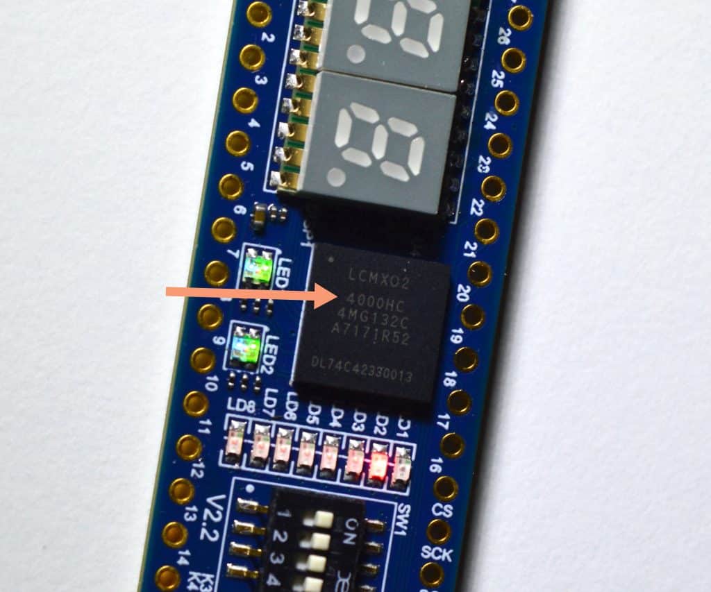
The specific board that I have been using is the STEP MX02 V2 board, which contains the MACHX02 FPGA chip from Lattice Semiconductor.
I am interested in FPGAs because they offer the easiest way to design and deploy custom integrated circuits.
But, let’s take a step back and ask an important question: What is an FPGA?
What is an FPGA?
A Programmable Field Gate Array is an integrated circuit that the end-user can configure after leaving the manufacturing plant. That is the meaning of the word “field” in its name.
This is in contrast to “regular” integrated circuits, like a microcontroller. With a microcontroller, like the Atmega328 in the Arduino, you can program by changing the contents of its application memory. By changing the application memory contents, you can change how the microcontroller behaves and what it does. However, the internal structure of the microcontroller, how its logical and functional components are organized and connected is not changed (and it can never be changed).
With an FPGA, on the other hand, programming affects the internal organization of the chip. An FPGA does not have a “program memory.” Instead, an FPGA consists of programmable logic blocks, and programmable interconnects. When you program an FPGA, you change how these interconnects are used to wiring the chip’s various functional components.
These logic components can be things such as:
- Logic gates, like “AND”, “OR”, “NOT”,
- Memory elements, such as flip-flops,
- Functional components like half-adders and full-adders,
- “hard blocks” like multipliers, digital signal processors, and input/output logic, and even full processors,
- clock infrastructure that can be used to synchronize various parts of a custom design.
So, think of an FPGA as a chip that contains logic components that can be wired and re-wired by you, the designer, with the ease of an Arduino.
FPGA programming: what is it like?
For someone used to “traditional” programming languages like Python and C, FPGA programming seems counter-intuitive.
First of all, to program an FPGA you will need a domain-specific programming language. Verilog is an excellent (and popular) choice and my specific choice. I’ll write more about Verilog later in this article.
You will also need a programming tool. The tool you use is typically dictated by the manufacturer of the FPGA chip you have chosen. For my STEP MX02 V2 board which contains the Lattice MachX02 FPGA, the programming tool is the Lattice Diamond editor, free to use and available only on Windows.
Now, what about my experience as a newbie in all this?
I must say, it was not an easy “getting started”.
Habits and knowledge that make me productive and comfortable in one domain, make it hard to learn new tricks that apply in a new domain.
For example, I am used to programs being executed one line at a time, from top to bottom. FPGAs don’t work like that. While you can control when things happen, but by default, everything happens at the same time.
I am also used to things like variables, data types, control structures, and all of the typical structures and features that most programming languages share. It is these common features that make it relatively easy to jump from one language to another without having to re-learn everything.
In a “regular” programming language I am used to working with bytes, integers, chars, and arrays. There is no such thing in Verilog (as far as I know).
There is only one “data type”: the bit.
A data type in Verilog exists to represent a value stored in a bit (of a flip-flop or wire), and the bit can have four possible values: 1, 0, x (an unknown value that can be 1 or 0), or z (a high-impedance state). While some of this may sound familiar (such as the first four possible values of a bit), the last one is probably not.
There’s more.
Consider that essentially, a Verilog program is an abstraction of a circuit. How do you make this abstraction real? How do you connect a construct of your Verilog program to something physical, like a pin of your FPGA chip?
For this to happen, you will need to implement some kind of mapping between the abstract (Verilog) and the concrete (FPGA).
All of the above can be done via the integrated programming tool (Diamond), but only after you let go of what you have learned about software programming, and switch your context to hardware programming.
At first, this is a very difficult task to do. When I took my first few baby steps in the world of FPGA programming, I was overloaded with new terms, new tools, new ways of doing things that will feel alien. I suspect you will be overloaded too.
As often is the case, you can turn on your noise filters to the maximum. With your filters on, you can get rid of most of the noise that blocks you from learning, and concentrate on the few things that really matter.
In my experience, I found that you can do interesting things with an FPGA without a 5-year degree in computer engineering.
The beginner’s process of programming an FPGA
After much deliberation (a.k.a. “frustration”), I have distilled the minimum viable process for programming an FPGA. In my experiments, I used the Lattice Diamond programming environment, Verilog, and the STEP MX02 V2 FPGA board. I’m sure you can use the same process with other FPGA programming environments, boards, and HDLs.
Here it is:
- Code the hardware logic in Verilog (“programming”). This is where you program the logic that will be implemented in the FPGA.
- Integrate the file (a.k.a. “synthesis“). This is where Diamond converts your Verilog program into a symbolic netlist. With this, you can see your program in a graphical view, with primitives (gates, clocks, logic components), wires, and ports.
- Assign pins. This is where you assign FPGA chip pins to Verilog ports. With this, your design can be implemented.
- Export your design to the FPGA chip. This is where you implement your Verilog program in hardware so that it can run on the FPGA chip.
This process omits a few additional steps that a professional Verilog engineer would include in her process. For example, an common step after the pin assignment step is to simulate the design before exporting it. Simulation gives us the opportunity to test the design for bugs and performance. But for my purposes of making progress with FPGA programming, it is not needed.
- Programming in Verilog. This is how you can design the logic that is eventually implemented in the FPGA. In my experience, learning the basics of Verilog was the hardest part of learning how to program an FPGA.
2. Synthesis is an operation that your FPGA programming tool will do automatically. With synthesis, your Verilog program is converted into a logic gate design implementation file that can be mapped onto the elements of the FPGA chip.
3. Assign pins. The logic you design in your Verilog program communicates with the outside world via ports. In this step, you assign physical FPGA chip pins to the logical ports. Your chip logic is now ready to deploy to a real FPGA chip.
4. Export your design to an FPGA chip. Just connect your FPGA board to your computer via USB, and click on the “program” button. No other programming hardware is needed. Wait for a few seconds for the process to finish, and boom, you have an operational custom FPGA chip.
This doesn’t seem so hard after all, right?
Yes, I agree.
Fundamentally, these four steps represent the minimal steps that you (or your programming tool) must do in order to program an FPGA chip. Contrast this to your Arduino experience, where you can shrink it down to steps 1 (write your program) and 2 + 4 (compile ~ synthesis and export).
In the case of FPGA programming, because of the abstracted nature of Verilog, we really need step 3 so that we can connect Verilog’s abstract ports to FPGA chip real pins.
That’s it!
Yes, there is a lot going on that you will need to eventually learn. Verilog, like Python, is easy to get started with, but has a lot of depth and complexity that allows you to create advanced chip designs. Lattice Diamond, too, is a complicated tool, much more complicated than the Arduino IDE, that professional chip designers use to create some of the chips that are in your computer right now.
But to get started, you don’t need any of that complexity.
Just these four steps.
How about we apply these steps in a couple of examples?
Example 1: Simple gate programming
Let’s look at a first example in which I will demonstrate how to write a very simple Verilog program that implements a simple AND gate. The AND gate receives input from two of the four switches available on the STEP MX02 V2 board, and “prints” the output to one (of eight) red LEDs.
If you are not familiar with the AND gate, check out this article (Wikipedia).
Here is an AND gate:
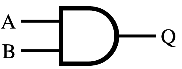
An AND gate operates by calculating an output depending on the values of the input, as per this truth table:
| A | B | Q |
|---|---|---|
| 1 | 1 | 1 |
| 1 | 0 | 0 |
| 0 | 1 | 0 |
| 0 | 0 | 0 |
For Verilog, this is a very simple operation, and can be written in a few simple lines of code. You should be able to understand what is going on in the code below even if you have never seen another Verilog program.
In this example, I will show you the process of programming the FPGA in detail, from start to finish. You can also watch the video below if you prefer (but best to both watch the video and read this article to get all of the details).
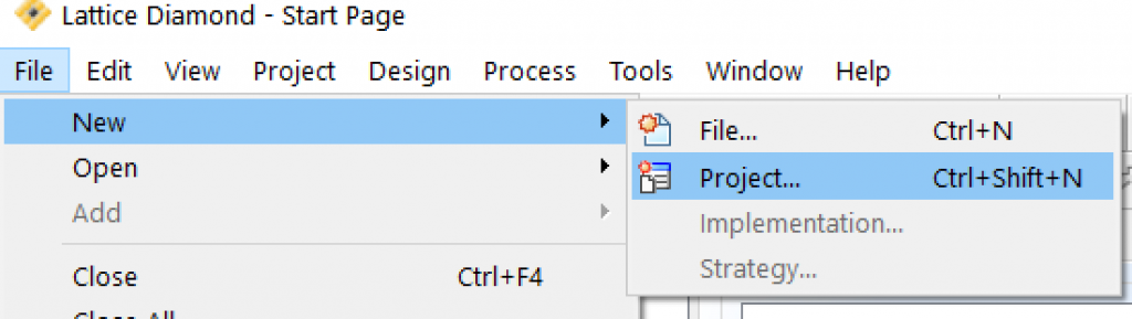
Step 1: Create a new project
Start by creating a new project in Lattice Diamond. Start Diamond, then click on File –> Project…
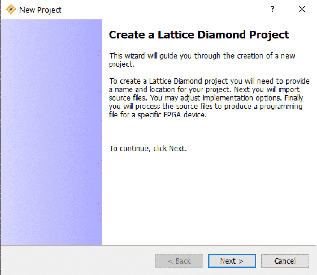
A “wizard” series of dialog boxes will help you with this process. In step 1, just click on “Next”:
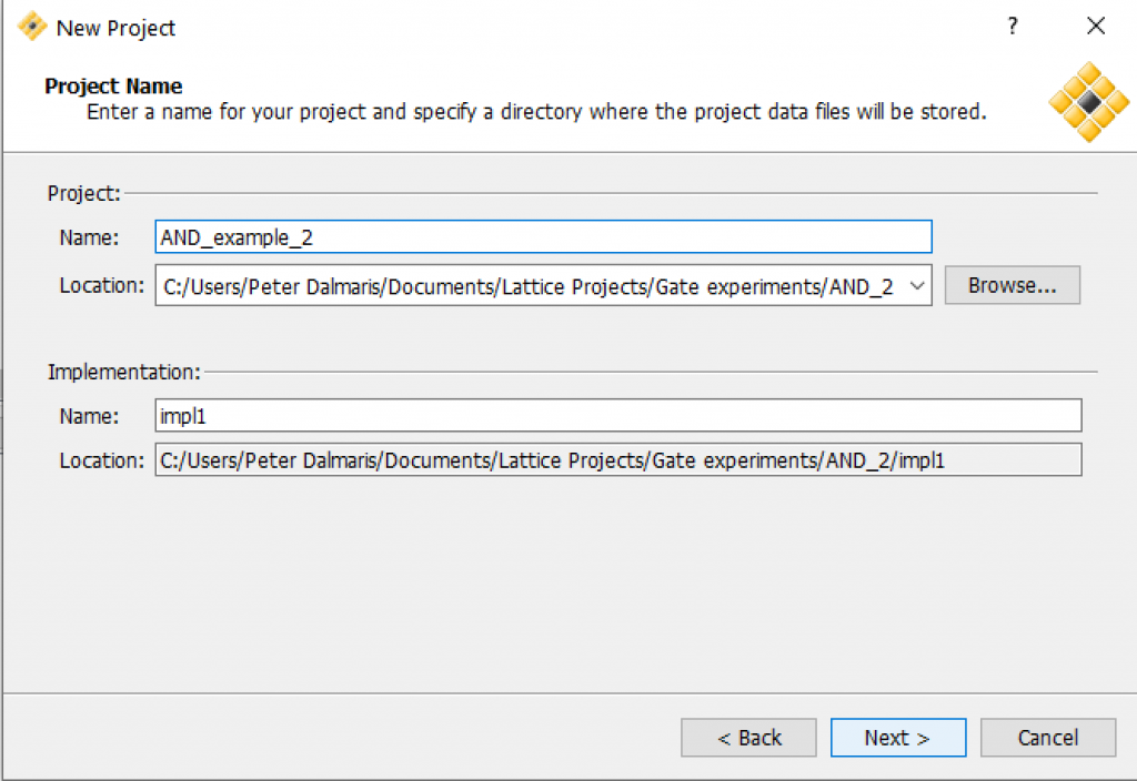
Now, give your project a name, and a location. In the implementation segment, you can leave the default name or change it to something more memorable. I also change the implementation location to be the same as the project location.
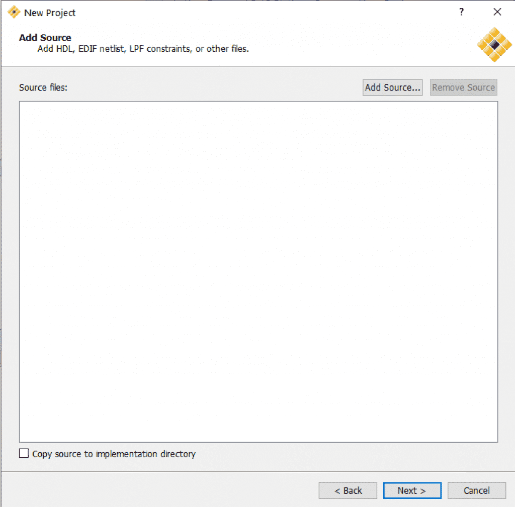
In step 3 you can add external sources (similar to libraries in Arduino C or modules in Python). We don’t have any in this example, so you can click Next.
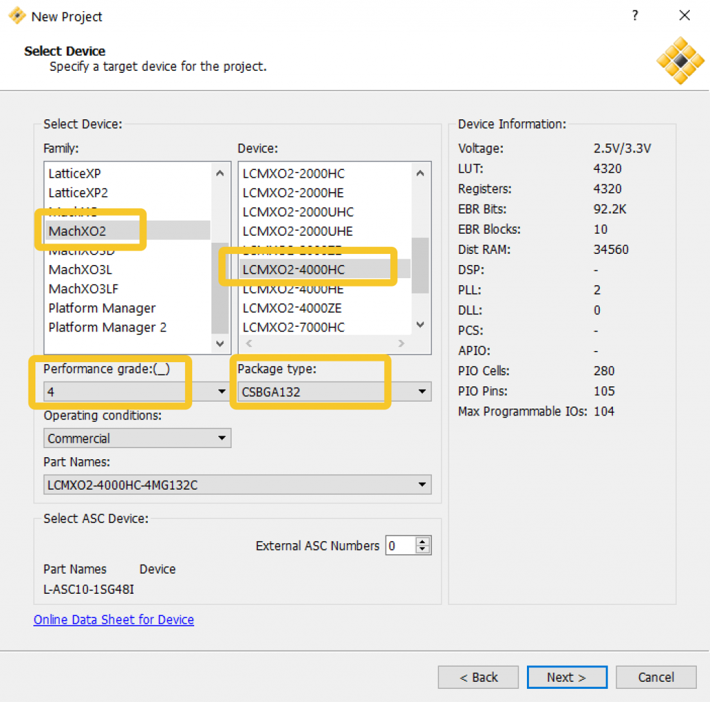
For the next step you will need hardware information about the FPGA chip you are using. My STEP MX02 V2 board contains the LCMX02-4000HC FPGA on a CSBGA132 package:
With this information, fill in the device information as in this example:
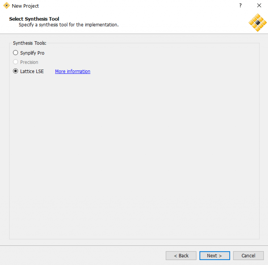
Next, we have the synthesis tool. I’ll be using Lattice LSE, so select this from the available options:
To finish the project creation wizard, click on Finish:
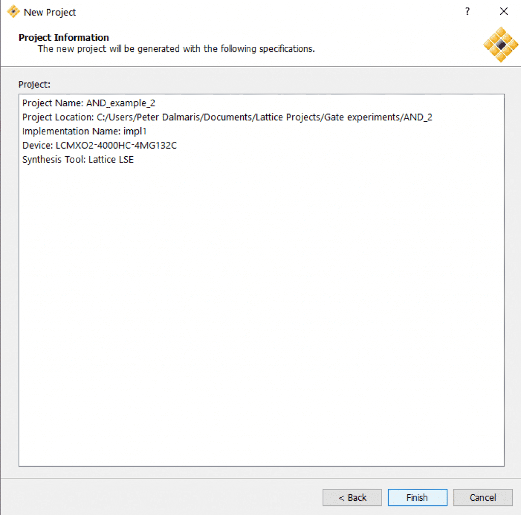
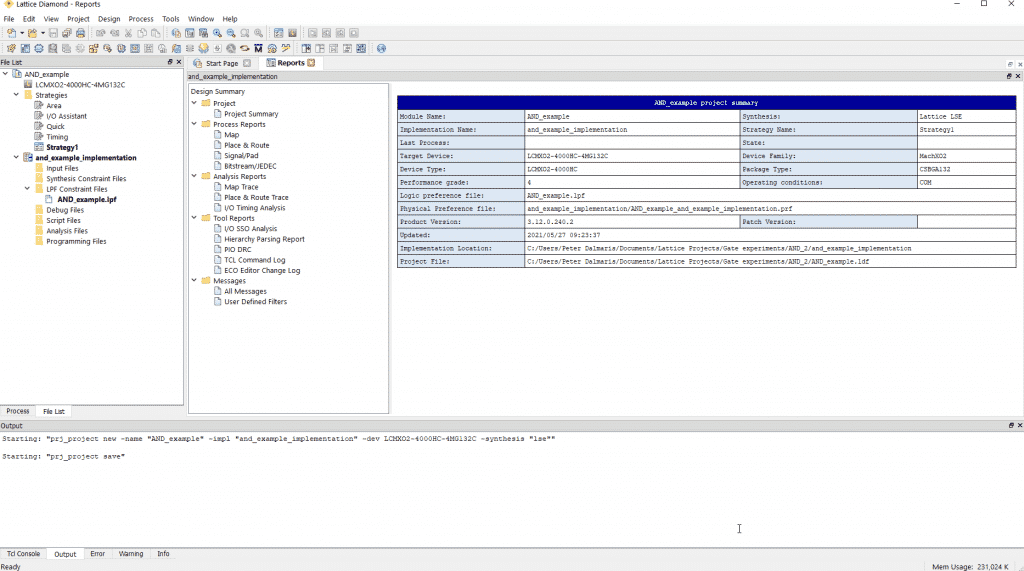
Your project is now ready. Lattice Diamond will show you a summary that looks like this:
Let’s continue with the Verilog program.
Step 2: Create the Verilog program.
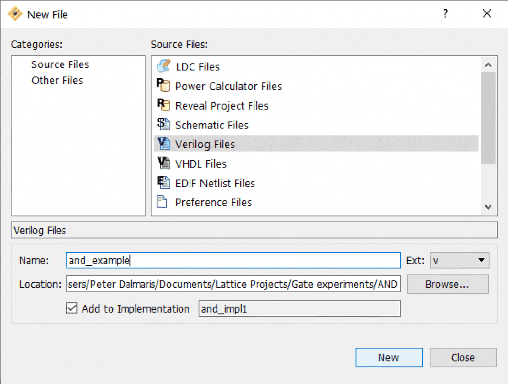
To create a new Verilog program file, click on File –> New, select “Verilog Files” as the source file, give it a name, and a location, and click on New:
Here’s the program:
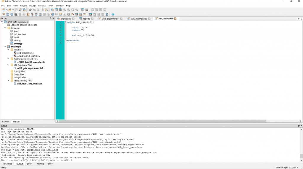
module AND_2(A,B,Y);

 input  A, B;  // Inputs for the AND gate
 output Y;     // Output for the AND gate

 and and_2(Y,A,B); // Implementation of the AND gate
                   // Using the "and"

endmodule
How simple is this?
The code is contained within the “module” and “endmodule” keywords.
I have named the module “AND_2“, which is my convention to signal that this module implements an AND gate with two inputs. In the parentheses, I list the ports that I’ll be using within the module: “A”, “B”, and “Y”. I have chosen to use single-letter names, but I could have gone with something more descriptive, like “input_1” and “input_2”. In the header, there is no differentiation between the types of ports I’m using (inputs, outputs, bi-directional).
Modules are like functions. You can create them and use them in other parts of your program. You can also use built-in modules, like “and” and “or”. This is what I do later in the program.
Note: Verilog is case-sensitive. "AND_2" is different to "And_2".
After the declaration, I define the types of ports I am using in the program. Ports “A” and “B” are inputs, while “Y” is an output.
Next, I instantiate the build-in module “and“, and declare it under the custom name “and_2”. The “and” module requires three parameters: first, the output, and second and third, the two inputs.
Verilog includes many modules that you can include in your programs, like “and”, “or”, “xor”, “nor”, and many more.
You can also find modules for flip-flops, latches, counters, shift registers, adders, multiplexers, and much more.
Once you write this program to the text editor in Diamond, it will look like this:
Step 3: Synthesize.
The next step is to synthesize the program. This is the equivalent of the “compile” step in Python or C programming, which converts a program from human-readable text to code that is executable by a CPU.
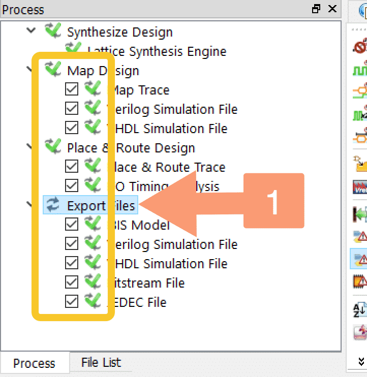
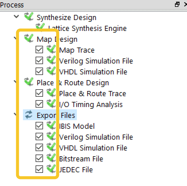
In Lattice Diamond, you can synthesize the program by double-clicking on the “Synthesize Design” header of the “Process” tab. Click on “Process” (1) first, then double-click on “Synthesize Design” (2) to start the synthesis process. Ensure that all the check-boxes are selected so that the relevant files are created. Don’t worry about what each of them does (not all of them are necessary, but that’s OK for now).
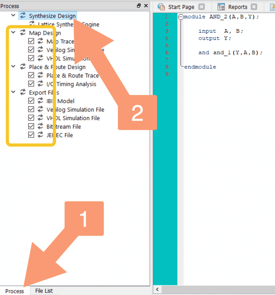
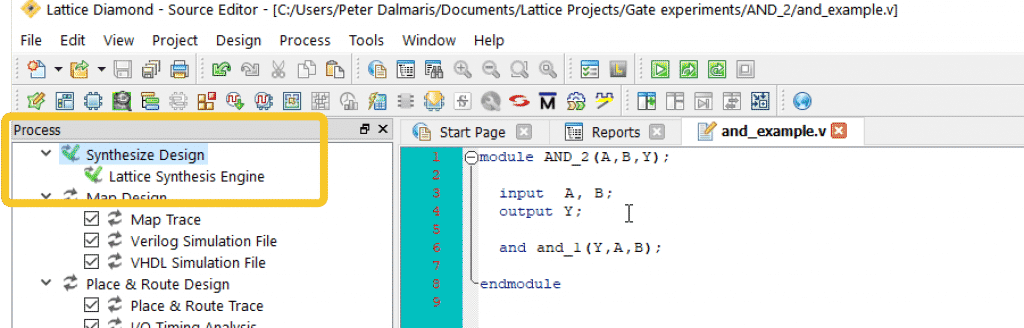
When synthesis is complete, you will see green tick marks next to the Lattice Synthesis Engine header, like this:
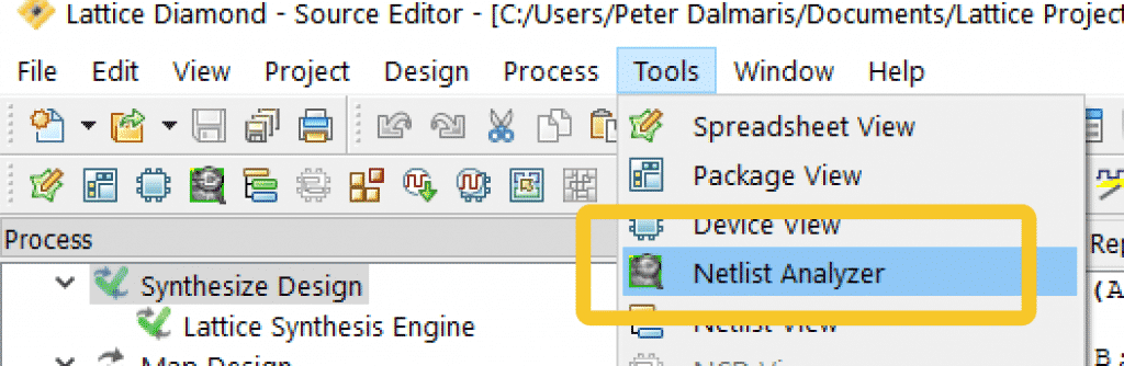
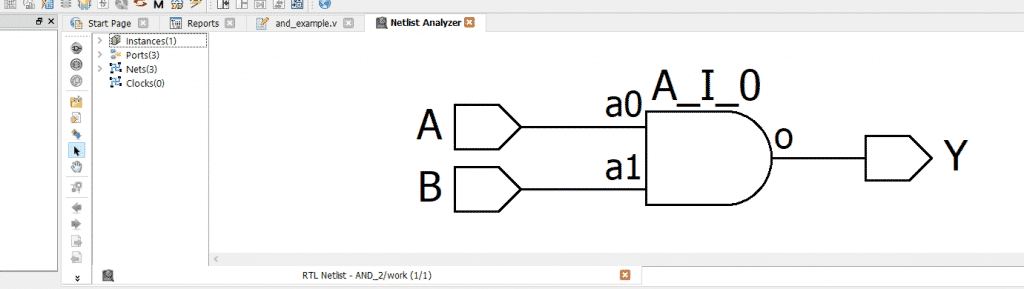
The synthesis engine has generated the project’s netlist. You can see a symbolic representation of your project by bringing up the Netlist Analyser. Click on Tools, then Netlist Analyzer to do this:
Here is a graphical representation of your project. The “and” module is depicted by the AND logic gate symbol, with its inputs and output:
Step 4: Assign pins.
The Verilog program is ready to be connected to the real world. We do this by assigning FPGA chip pins to the Verilog ports.
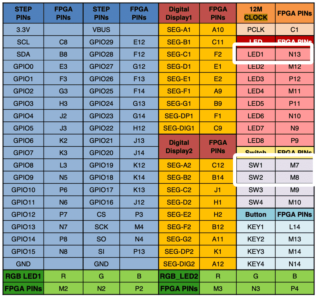
My STEP MX02 V2 board is equipped with convenient buttons, LEDs (including 2 RGBs), switches, and two seven-segment displays. I will assign two of the switches to serve as inputs to the AND gate, and one LED to be the output.
Here is a pin map for this device (taken from the documentation that ships with the module):
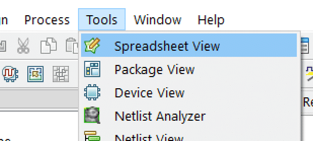
To do the pin assignment, select Tools, Spreadsheet View:
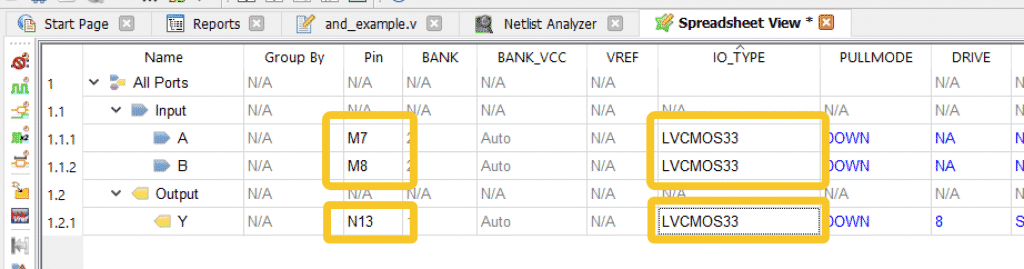
The Spreadsheet View makes it easy to assign pins to ports. You can see the ports in the left-most column, and several columns. You only need to be concerned with the Pin and IO_Type columns.
In the Pin column, type “M7”, “M8” and “N13” in the “A”, “B” and “Y” rows respectively. This assigns pin M7 (switch 1) to port A, pin M8 (switch 2) to port B, and pin N13 (LED 1) to port Y.
For the IO_Type, select LVVCMOS33 for all ports.
The spreadsheet now looks like this:
Step 5: Export files.
Before we can program the FPGA chip, we must export the necessary files. This is an automated process, triggered by a double-click on the Export Files header of the Process tab.
Go ahead and do this now. As the Export Files process runs, you will see green tick marks confirming success next to each file in the process tab.
We are now ready to program the FPGA.
Step 6: Programming.
It is time to “manufacture” your first integrated circuit — no need for a manufacturing plant. Manufacturing an IC with an FPGA (“programming an FPGA”) is something you can do with one click.
Start by connecting the STEP MX02 V2 board to your computer via USB.
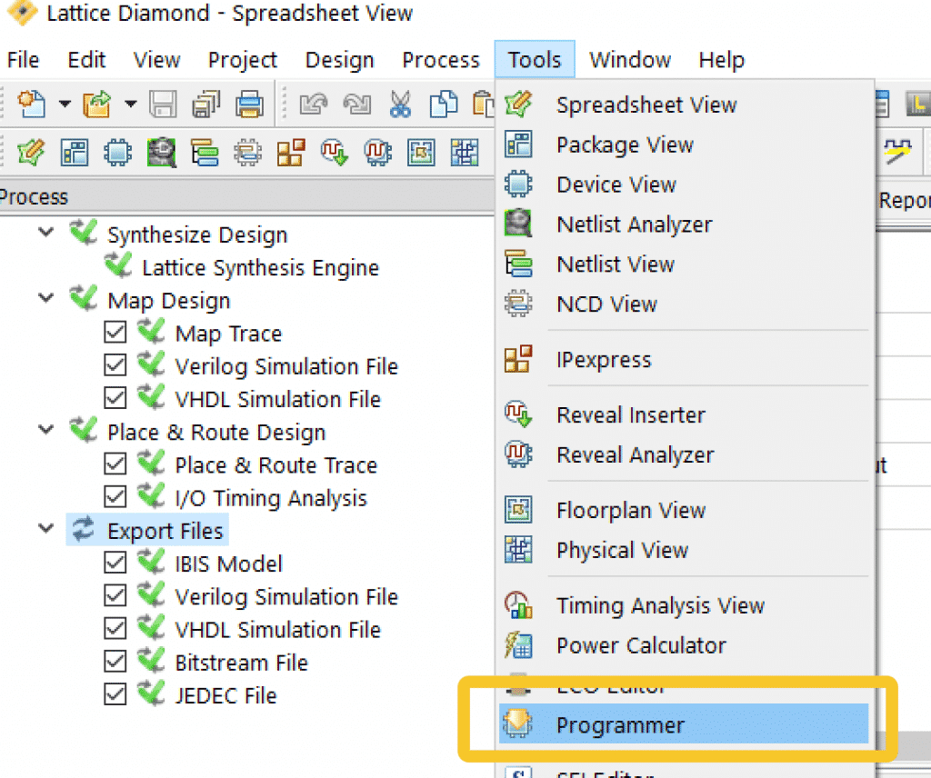
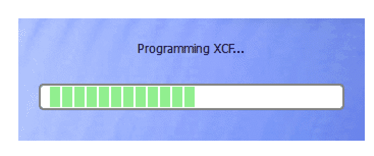
Then, bring up the Diamond programmer tool. Click on Tools, Programmer:
A dialog box will pop up. You must select the appropriate settings for the Cable and Port drop-downs, as per the screenshot below. Click on the “Detect Cable” button to confirm you have the correct settings:
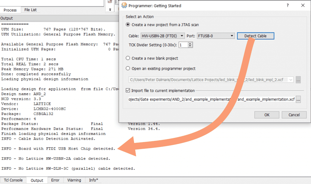
A new tab will appear in Lattice Diamond that contains the programming target, cable settings, and several new buttons. Inspect the cable settings to confirm they are correct, and then click on Detect Cable (1). You should see confirmation in the Output pane.
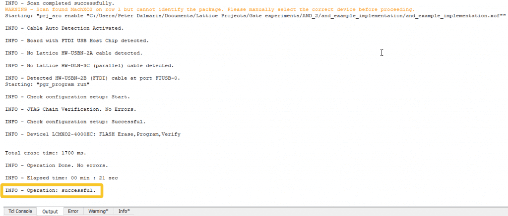
Then, click on the Program button (2) to start the programming. If you receive a complaint that the device target is incorrect, click on the drop-down under the Device column (3) to select the correct device and then click on Program (2) again.
You will see a progress bar and relevant information in the Output pane. Once the programming is complete, the message “Operation: successful.” will appear in the output.
That’s it. You have created your first custom integrated circuit!
Step 7: Testing.
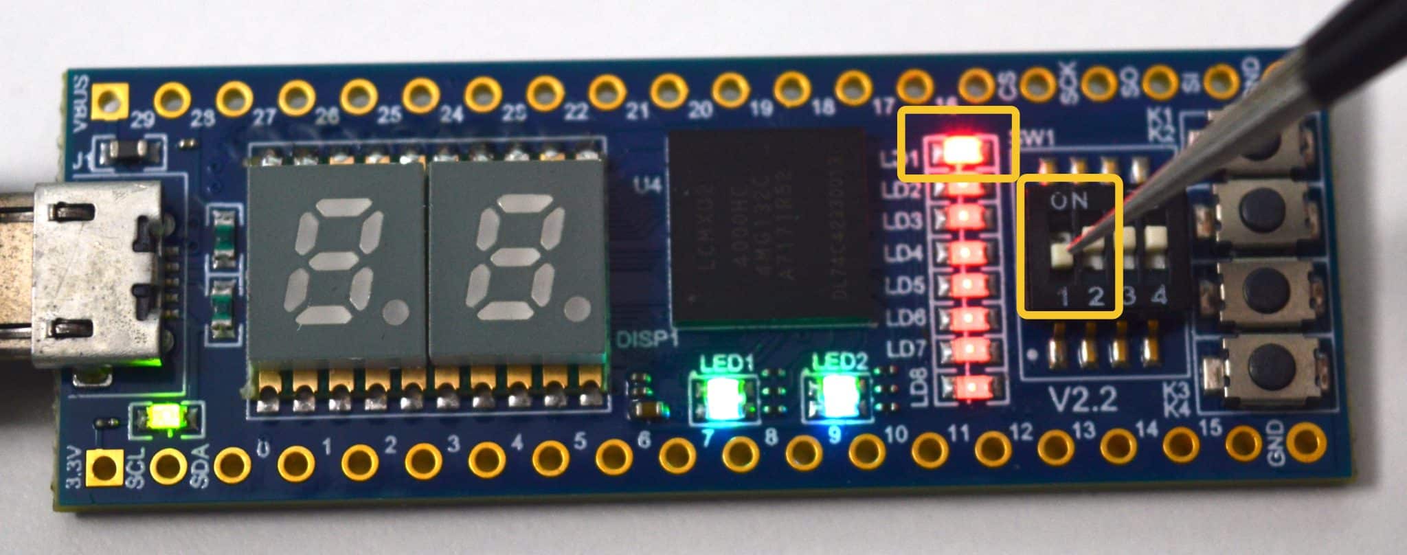
Let’s make sure that the programmed FPGA chip works as expected. You will need an object with a fine tip to help you manipulate the tiny switches on the STEP MX02 V2 board. I’m using a pair of fine tweezers.
Remember the truth table for the AND gate that I mentioned earlier? I will edit it to better reflect the position of the switch and the state of the LED. This will make it easier for me to confirm that the implementation of the AND gate on the FPGA chip works.
| SW1 | SW2 | LD1 |
|---|---|---|
|
|
|
|
|
|
|
|
|
|
|
|
|
|
|
|
In this table, for the inputs, logical “1” is the “Up” switch position, and logical “0” is “Down.” The LED output, logical “1” is when the LED is off, and logical “0” is when the LED is on. This may feel counter-intuitive, but it is due to the way that the LED is connected. If you want to get a more intuitive outcome, where an LED that is turned on represents logical “1”, you can change the “and” gate for the “nand” gate (not-and).
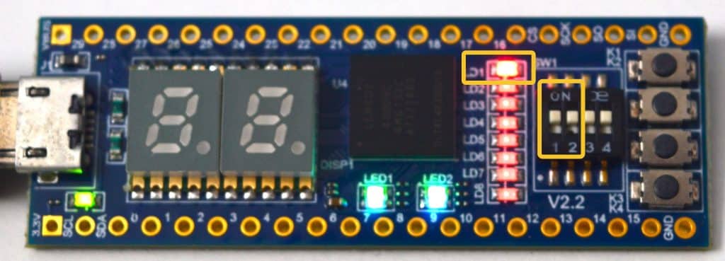
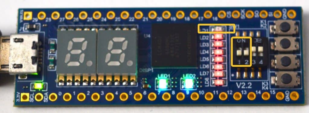
Now, let’s try out various switch positions and the output they create on the LED. The following photos contain the results of my experiment:
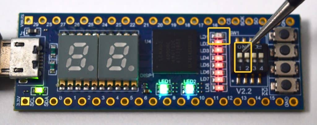
UP, UP –> OFF 
DOWN, UP –> ON
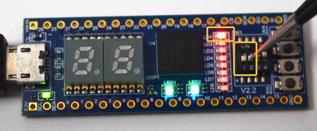
DOWN, DOWN –> ON 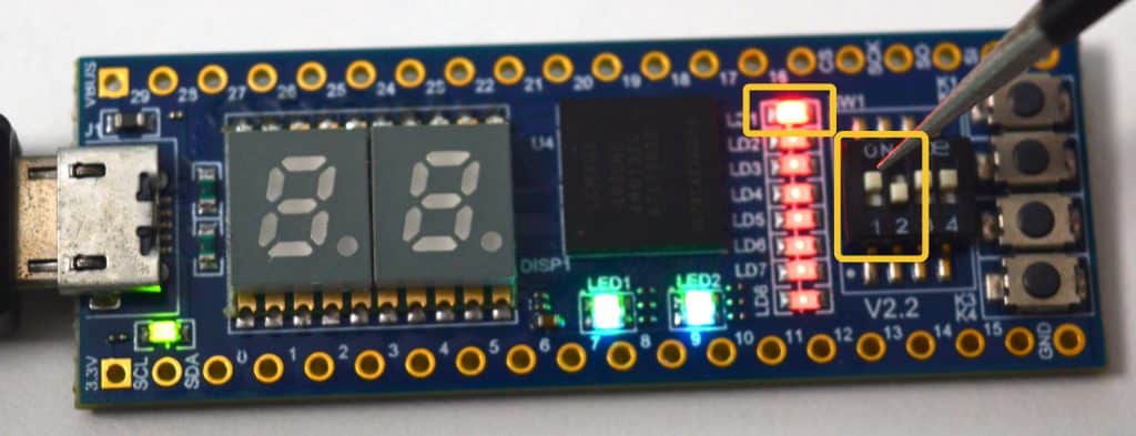
UP, DOWN –> ON

Note: In the photos above, you can notice the the LEDs (other then LED 1) are in neither on or off. They are in an undefined state because in our program we have not set them to a particular state. This is not a problem for the purposes of this demo, so you can safely ignore them.
Iterative development
FPGA programming with an editor like Lattice Diamond allows you to iterate through versions of your design easily. Let’s look at a quick example.
Say that you are not satisfied by how the LED responds to the position of the switches. At the moment, when both switches are turned on, the LED is off.
Would you prefer it if the LED was on when both switches are on?
No problem.
The easiest way to deal with this is to change the “and” gate to an “nand” gate.
Go back to your Verilog program and edit it to look like this:
module AND_2(A,B,Y);

 input  A, B;  // Inputs for the AND gate
 output Y;     // Output for the AND gate

 nand nand_2(Y,A,B); // Implementation of the AND gate
                   // Using the "and"

endmodule
I have marked the changes with bold text.
To test the new behavior of your FPGA board, repeat steps 3 (synthesis), 5 (export), and 6 (program). There is no change in the pin assignments, so no need to re-do step 4.
Now checkout how the LED behaves against the four possible switch combinations. Photos are below:
UP, UP –> ON 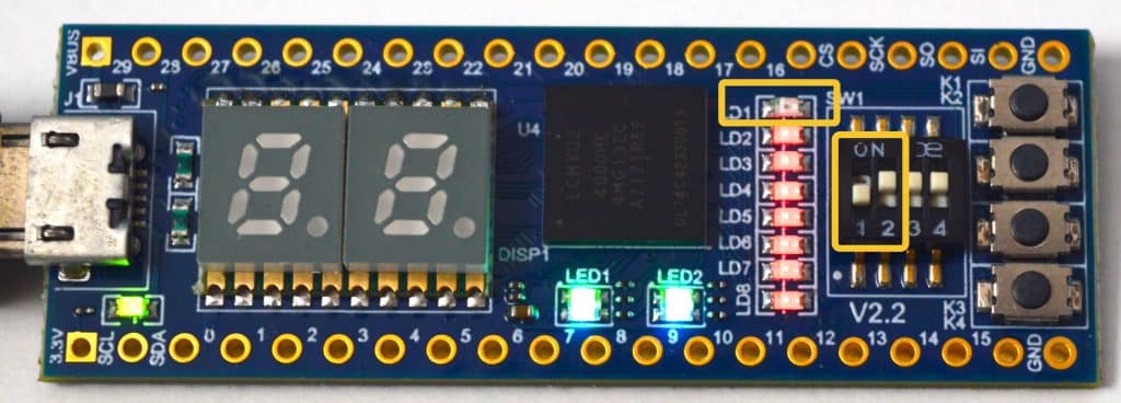
DOWN, UP –> OFF
DOWN, DOWN –> OFF 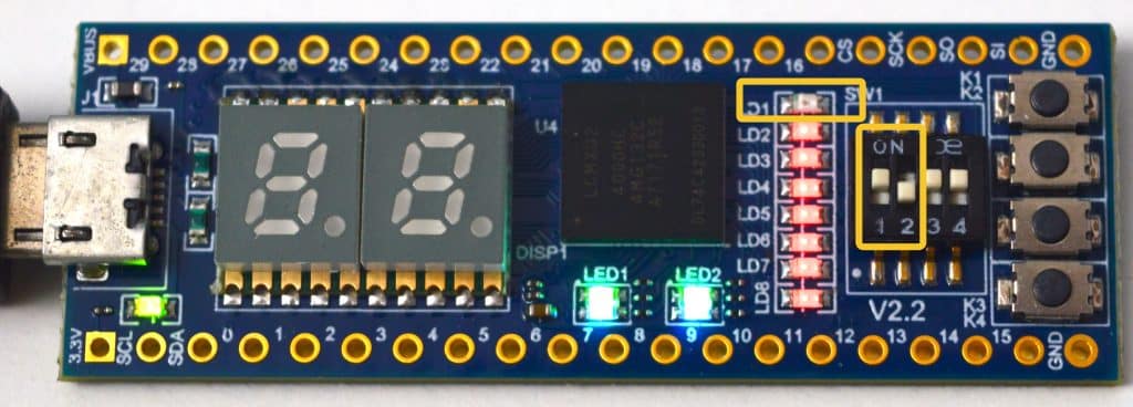
UP, DOWN –> OFF
Below is the truth table that matches the new iteration of the program (using NAND instead of AND):
| SW1 | SW2 | LD1 |
|---|---|---|
| UP | UP | ON |
| UP | DOWN | OFF |
| DOWN | UP | OFF |
| DOWN | DOWN | OFF |
This was my first Verilog program and the first one to deploy on my STEP MX02 V2 board. I continued with a few similar experiments that involved other logic gates and played with a few combinations.
But then, I wanted to try out the traditional “blinking LED” experiment.
Example 2: Simple blinking LED
Playing with gates is an excellent way to get started with Verilog and FPGA programming. Coming from the Arduino world, though, I was keen to figure out how to make an LED blink. This would allow me to learn how to use an external LED (in addition to the ones included in the FPGA board) as timers.
I am documenting the process below, but I will not detail anything that I have already explained earlier for the benefit of brevity.
Let’s start with the hardware, and then continue with the software. You can also watch the video below if you prefer (but best to both watch the video and read this article to get all of the details).
Step 1: Hardware
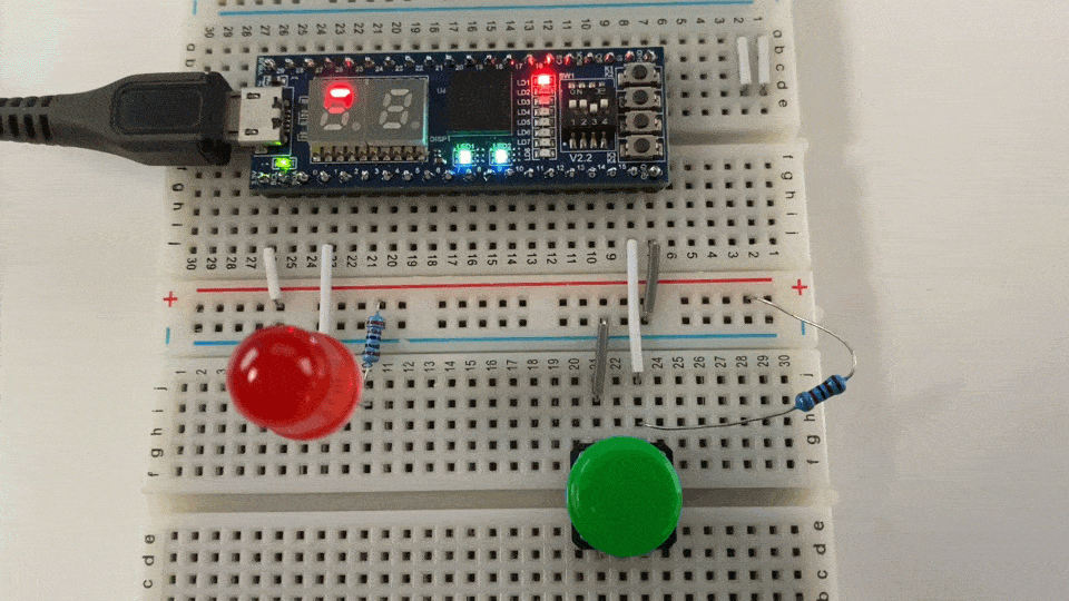
Here’s a photo of the circuit:
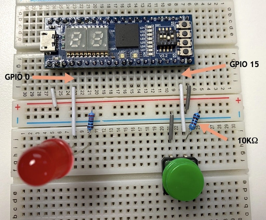
I have combined two mini breadboards to make wiring more comfortable. I use the STEP MX02 V2 board to control the LED.
The left-most pin of the row that is closer to the visible power rails provides 3.3V, so I have connected it to the red power rail. The right-most pin on the other side is GND and is connected to the blue power rail.
For the LED, I have connected its cathode to GPIO 0, and its anode to the red power rail via a 10KΩ resistor.
I’m also using a button to reset a counter used in the program. The right pin of the button goes to GPIO 15, and the left pin goes to the blue power rail (GND). I have also attached a 10KΩ pull-up resistor between the right button pin (signal) and red power rail (3.3V).
Let’s continue with the software.
Step 2: Create a new project.
Connect your FPGA board to your computer via USB, and start Lattice Diamond. Create a new project as per the previous demo.
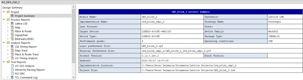
I named mine LED_blink_2.
Here is my project summary:
Step 3: Create the Verilog program.
This is the most interesting part of the process.
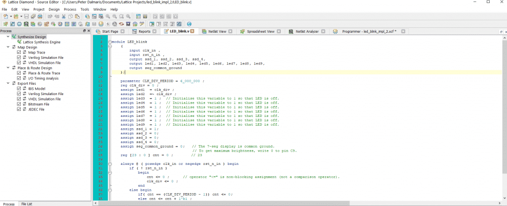
Create a new Verilog program file, and populate it with this code:
module LED_blink
  (
   input clk_in ,
   input rst_n_in ,
   output ssd_1, ssd_2, ssd_3, ssd_4,
   output led1, led2, led3, led4, led5, led6, led7, led8, led9,
   output seg_common_ground
  );

   parameter CLK_DIV_PERIOD = 6_000_000 ;

   reg clk_div = 0 ;
   assign led1  = clk_div ;
   assign led2  =~ clk_div ;

   assign led3  = 1 ;  // Initialise LED off.
   assign led4  = 1 ;  // Initialise LED off.
   assign led5  = 1 ;  // Initialise LED off.
   assign led6  = 1 ;  // Initialise LED off.
   assign led7  = 1 ;  // Initialise LED off.
   assign led8  = 1 ;  // Initialise LED off.
   assign led9  = 1 ;  // Initialise LED off.
   assign ssd_1 = 1;   // Initialise so SSD segment 1 is on.
   assign ssd_2 = 0;   // Initialise so SSD segment 2 is on.
   assign ssd_3 = 0;   // Initialise so SSD segment 3 is on.
   assign ssd_4 = 0;   // Initialise so SSD segment 4 is on.
   assign seg_common_ground = 0; // The 7-seg display is common ground.
                                 // To get maximum brightness, write 0 to pin C9.
   reg [23 : 0 ] cnt = 0 ;

   always @ ( posedge clk_in or negedge rst_n_in ) begin
     if ( ! rst_n_in )
       begin
         cnt <= 0 ;      // operator "<=" is non-blocking assignment (not a
                         // comparison operator).
         clk_div <= 0 ;
       end
     else begin
       if( cnt == (CLK_DIV_PERIOD - 1)) cnt <= 0;
       else cnt <= cnt + 1'b1 ;
       if ( cnt < ( CLK_DIV_PERIOD >> 1 ) ) clk_div <= 0 ;
       else clk_div <= 1 ;
     end
   end
 endmodule
There’s a lot of new instructions in this code, so let’s go through an overview.
The program starts with the module keyword, and a name for the module. I called this block “LED_blink”.
Following that is a list of ports. Because this program has a long list of ports than the example of demo 1, I chose to declare these ports below the module keyword AND to declare their type in addition to their name.
The program will only manipulate a few of these ports, but I have declared additional LEDs to initialize them (instead of leaving them in an undefined state, as in demo 1).
Next, I’m using the “parameter” keyword to create a constant. I’ll use this constant later in the program to control the frequency of the LED blinking. The FPGA board I am using has a core clock frequency of 12MhZ. I intend to blink the LED at a frequency of 2Hz. Therefore I must divide the core frequency by 6MhZ to achieve that.
In the next line, I use the “reg” keyword to create the equivalent of a variable. This variable can hold a 24-bit value, hence the notation [23:0]. In the pin assignment step, I’ll be linking this variable to the FPGA clock, which yields 24-bit values.
The next 14 lines use the “assign” keyword to write a value to a wire. Take this example:
assign led3 = 1 ;Here, the wire “led3” is given a constant value “1”.
In this example, on the other hand:
assign led1 = clk_div ;… wire “led1” is given the value stored in the variable “clk_div”.
Think of these “assignments” as wires that propagate a value. You could use them to link to ports together, a port to a constant value, or a port to the output of a module (such as a timer module).
The value that is written to a wire can also be an arbitrary expression that consists of other wires or variables.
They are evaluated in parallel, not in series as in a “regular” program.
In this example, the only active ports are LED1, the external LED (we’ll connect it to GPIO15), the external button (we’ll connect it to GPIO0), and one of the segments of the 7-segment display. For the reset, I’m simply tying them to a stable state to keep them turned off.
Unlike the “assign” keyword, the “always” keyword allows you to create a block of code where instructions are executed sequentially, like in a regular program.
In this example, the code inside the “always” block is triggered by a transition of the clock signal. This transition can be the signal’s positive or negative edge. The condition inside the parentheses of the “always” block is known as the “sensitivity list.”
Inside the “always” block, you can see several “if” statements and blocks defined with the “begin” and “end” keywords. This code determines the values that should be written to the led1 and led2 wires (which we’ll connect to the two LEDs later).
A few things to keep in mind:
- The “!” operator will convert a non-zero value to zero, and vice-versa.
- The “<=” operator will write a value to a variable (not to be confused with “=”), and in this context (not a comparison) is not the “less-then-or-equal” operator. Learn more.
- Operators used inside an “if” keyword, like “”==” and “<“, are regular comparison operators.
Let’s continue.
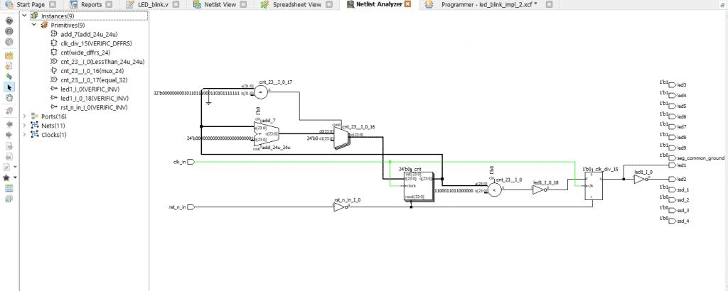
Step 4: Synthesize.
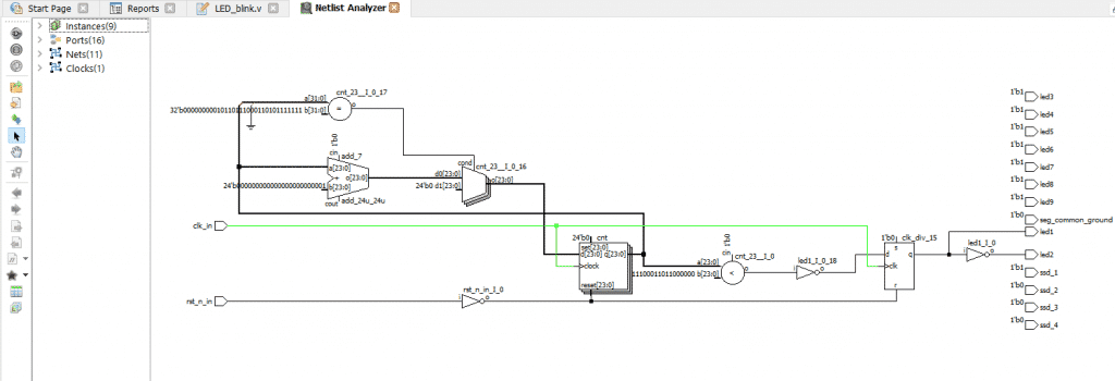
Double-click on the “Synthesize Design” header in the Process pane to run the synthesis tool.
You can see the result in the Netlist Analyzer:
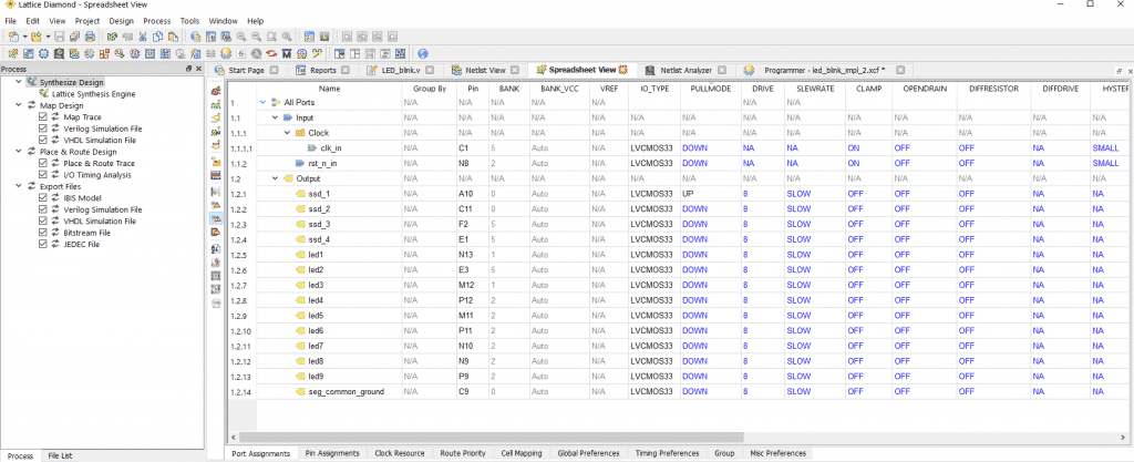
Step 5: Assign pins.
Let’s assign pins to ports. You can see my assignments in the screenshot below.
For any column that is not visible in the screenshot, you can retain the default values.
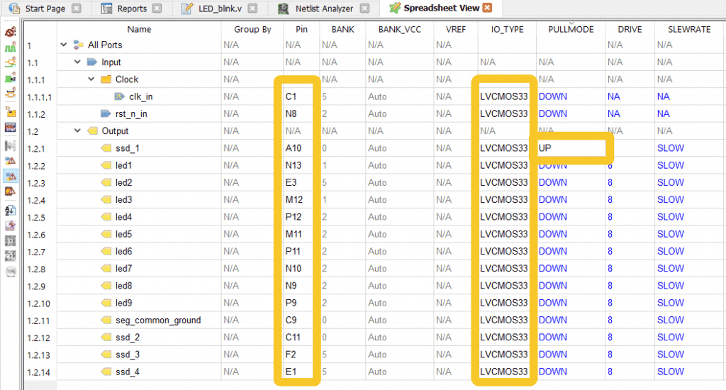
Note: Notice that the PULLMODE value for ssd_1 is UP.
Step 6: Export files.
Go ahead and export the files by double-clicking on the Export Files label (in the Process pane).
You should see green tick-marks, like this:
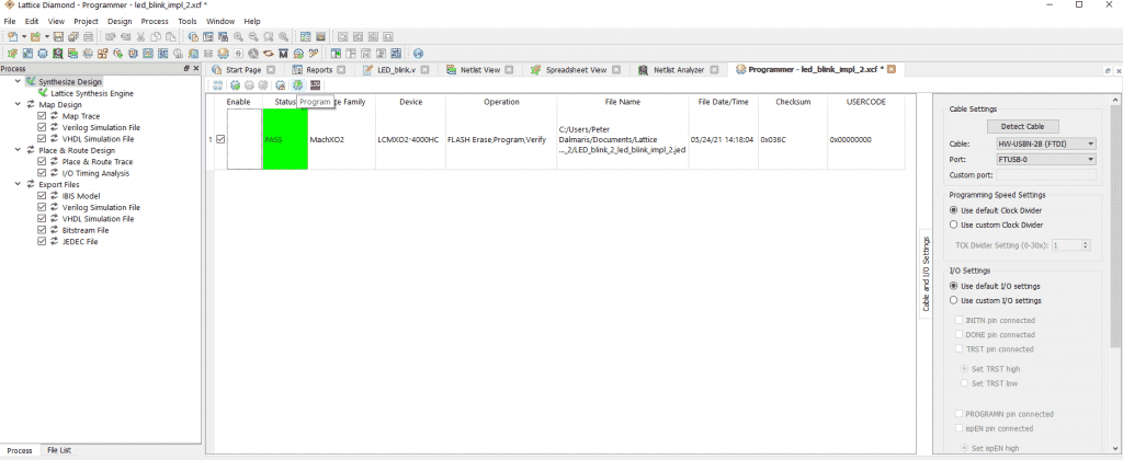
Step 7: Programming.
Almost done, let’s do the programming.
Bring up the Programmer tool (Tools, Programmer), and click on Detect Cable (under Cable Settings) to ensure there is a connection with the FPGA board.
Then, click on the Program button. You should see the progress bar:
Lets’ test!
Step 8: Testing.
The on-board LED1, and external LED should be blinking in turn: onboard –> external –> onboard –> external etc.
You can reset the program by pressing the external button.
One of the segments of the 7-segment display should also be lit.
Here’s an animated GIF the show the outcome of this experiment:
Awesome?
Isn’t this awesome?
OK, it’s just a blinking LED effect…
But it’s done by an integrated circuit that you have designed. There is no firmware running on this chip (as it does with a microcontroller), but the custom configuration of the FPGA chip.
The same process is used to design far more complicated integrated circuits, from simple gate arrays to CPUs.
Are you interested to learn more about FPGAs?
Why?
Let me know in the comments.