9. A hands-on tour of KiCad with a very simple project
Layout in Pcbnew
Pcbnew is KiCad’s layout editor. Think of it as a drawing program that is specifically designed for drawing printed circuit boards. Pick up a PCB and, and try to identify and list its most important attributes.
Your list should be similar to this:
1. Components, like resistors and integrated circuits,
2. Wires (or traces, as we will call them), that connect the components,
3. A board made of fibreglass or similar material, with a particular shape,
4. Graphics, like text or drawings, printed on the board,
5. Holes, large or small.
6. Components, wires, and graphics may appear on one, or two sides of the board. Wires can also appear in many layers that are sandwiched between the top and bottom layer to allow for more complicated circuits.
We use the layout editor to design a PCB with all of these elements. With KiCad’s Pcbnew, you can design PCBs that are very simple, like the one we are working on in this section, and extremely complicated and dense ones, like the one in Figure 9.1.
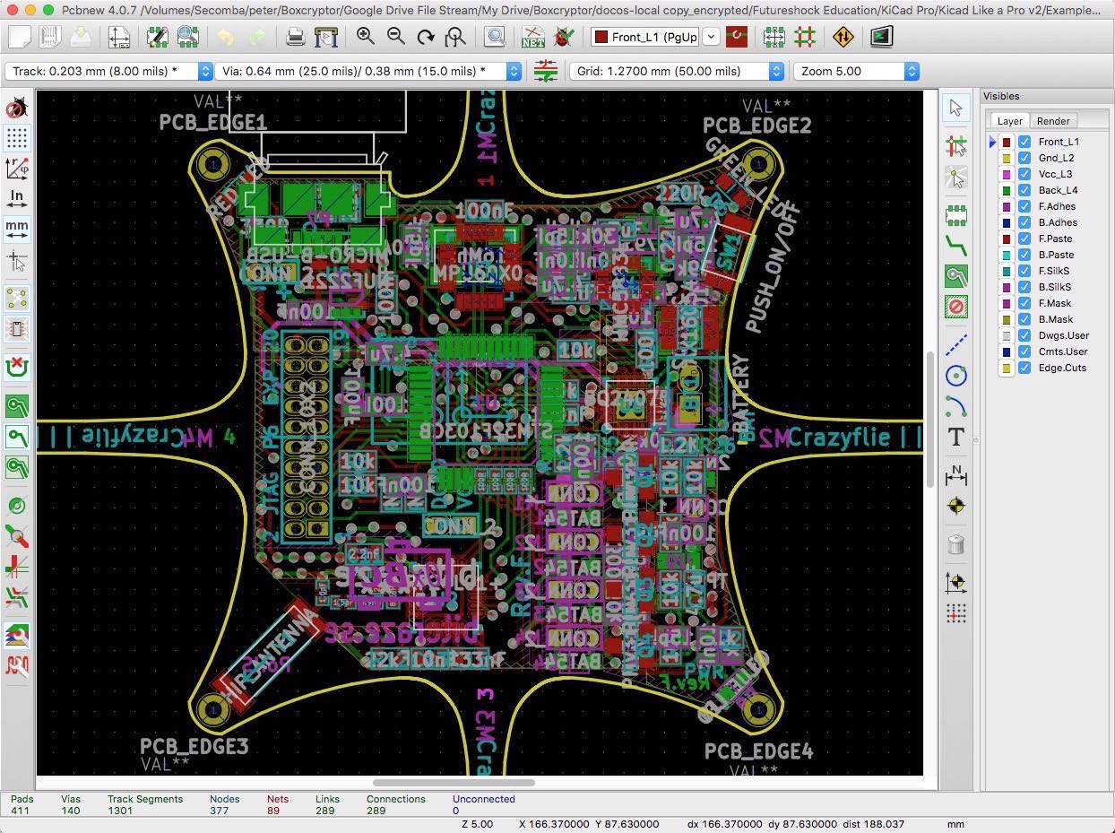
Figure 9.1: An example of a relatively dense layout in Pcbnew. It belongs to the Crazyflie project[4].
In the next few pages, you will take a hand-on tour of Pcbnew and learn about it most important features.
The user interface
Let’s start Pcbnew. The objective is to become familiar with its user interface and the functionality that is absolutely necessary for our very simple first project.
To start Pcbnew, go back to the KiCad main application, and click on the Pcbnew button, as in the example in Figure 9.2.
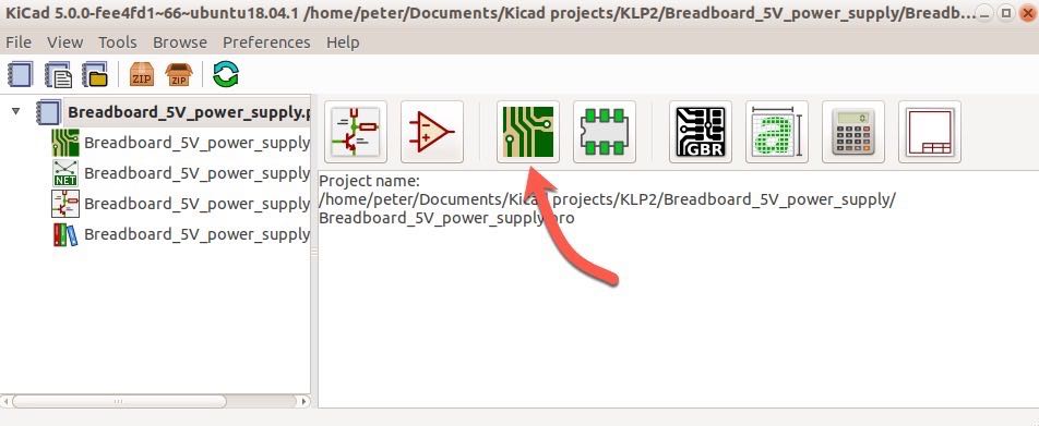
Figure 9.2: Start Pcbnew from the main KiCad application window.
You can also start Pcbnew through the menu. Click on Tools, and then 'Run Pcbnew', or through a keyboard shortcut (Ctrl-P on Windows and Linux, Cmd-P on Mac OS).
Pcbnew will start, and you will see the main window. It should look like the example in Figure 9.3.
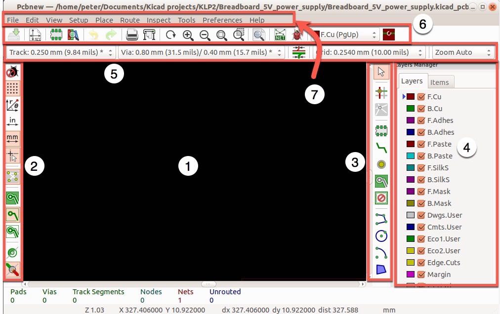
Figure 9.3: The Pcbnew main window, with its toolbars annotated.
Compared to Eeschema, Pcbnew may seem more complex and even intimidating, but rest assured, it isn’t. In this part of the book, I will help you to learn only the most important functionalities so that you can start designing your PCB very quickly. Just like we did in the Eeschema segment, we’ll start with the basics of the layout sheet (item 1 in Figure 9.3), then learn about the mouse and hotkeys controls, and then the toolbars and menu bars (the rest of the items in Figure 9.3).
Let’s start with the layout sheet.
The layout sheet
Similarly to Eeschema, in Pcbnew you design your PCBs inside the designated sheet area. It does look very similar to the schematic sheet. You can also edit the layout template in Pcbnew in the same way you did in Eeschema. That is, by editing the page layout description file using the Pl_editor application.
You can also load an existing custom layout exactly as you did in Eeschema. In Pcbnew, click on the File menu, then click on Page Settings. At the bottom right side of the window, you will see the 'Page layout description file' text field. Use the 'Browse' button to find and select the template you created earlier in this section.
While you have the Page Settings window open, let’s fill in the form so that it looks like the example in Figure 9.4.
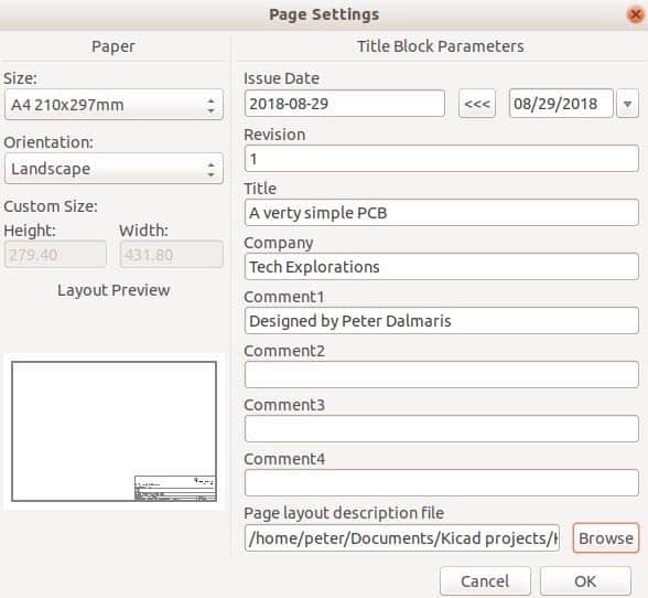
Figure 9.4: The Pcbnew Page Settings dialog box.
As you can see, the fields in the Pcbnew page settings window are identical to the ones in Eeschema. Click on the Ok button to commit the title block text, and confirm that your text appears in Pcbnew’s title block (as in the example in Figure 9.5).
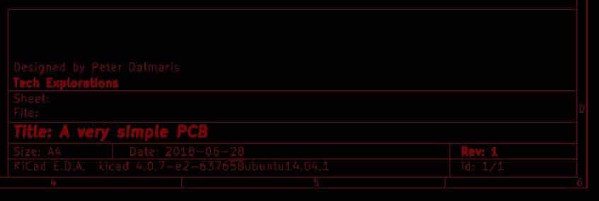
Figure 9.5: The Pcbnew title block.
The layout sheet uses a grid to help you place components on specific, evenly spaced, locations. You can control the size of the grid from the grid drop-down widget in the top toolbar.
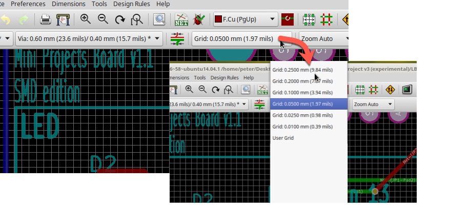
Figure 9.6: You can change the grid size from the Grid drop-down widget.
When you are working on loosely populated PCBs (like the one we are working on in this segment), you can opt for larger grids.
Another useful feature that you will use a lot, is called 'Zoom to Fit' (Figure 9.7).
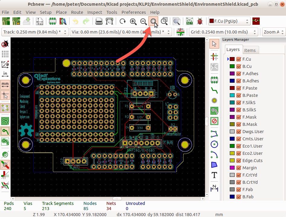
Figure 9.7: Zoom to fit changes the zoom level so that the entire PCB fits in the Pcbnew window.
When you click on the 'Zoom to fit' button, situated in the top toolbar, the zoom level of the sheet changes so that the complete PCB can fit within the Pcbnew window.
Mouse buttons and hotkeys
In Pcbnew, the mouse and hotkeys work almost exactly the same as they do in Eeschema. I use a mouse with two buttons and a scroll wheel. The scroll wheel is useful for zooming in and out of the sheet.
This table contains information about the default role of each button or button and key combinations:
Button, Keys |
Role |
Left mouse button (LMB), single click |
Show selected footprint’s details in the status bar |
Left mouse button (LMB), double-click |
Show footprints properties window for the selected footprint |
Right mouse button (RMB) |
Show the context menu for selection |
Alt/Cmd + Right mouse button (RMB) |
Pan (please note: this combination may be different for you, as it depends on how your mouse and keyboard are setup on your computer). |
Scroll wheel |
Zoom in/out at the position of the cursor |
Table 9.1: Mouse controls in Pcbnew.
When you do a single left click on a footprint, the footprint’s details are shown in the status bar, at the bottom of the Pcbnew window, like in the example in Figure 9.8.
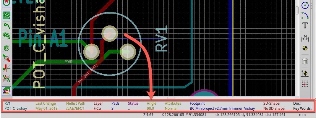
Figure 9.8: To see a footprint’s details, click on it.
In the example of Figure 9.8, I have left-clicked on the footprints of a potentiometer ('RV1'). In response, Pcbnew shows me the details of this footprint in the status bar, in the area inside the red box. From this, you can see the number of pads included in this footprint (3), it’s orientation (90 degrees from its default orientation), which library it belongs to ('BC Miniproject v2:7Trimmer_Vishay'), and more.
When you double left-click on a footprint, the Footprint Properties window for this footprint will come up.
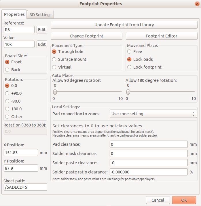
Figure 9.9: Double left-click on a footprint to open the footprint properties window.
In the footprint properties window, you can edit that footprint’s properties, such as its reference designation, its orientation, position, and much more. You can also change the association of the underlying component to a different footprint, or start the footprint editor so that you can edit the current footprint.
The right mouse button produces a contextual menu that depends on what you clicked on. For example, if you click on a footprint, you will get the context menu in Figure 9.10.
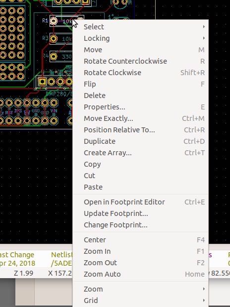
Figure 9.10: Clicking on a footprint produces this context menu.
Many of the functions in this menu are accessible through simple hotkeys, like 'E' for the Properties window, 'R' to Rotate, and 'M' to Move. These hotkeys should be familiar to you from Eeschema.
If you right-click on a track, you will get the context menu in Figure 9.11.
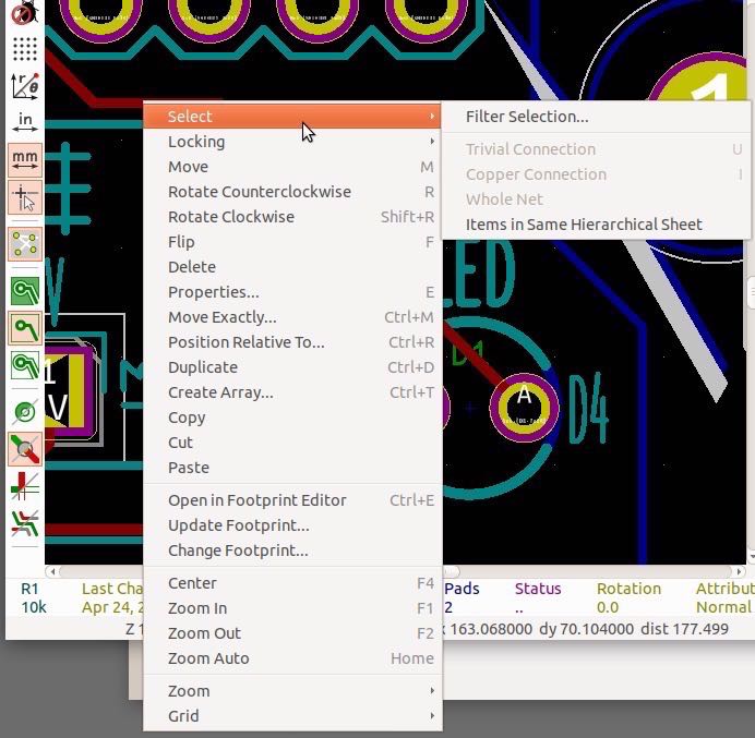
Figure 9.11: Clicking on a track produces this context menu.
Notice the there is very little difference between the two context menus. The track contextual menu contains the 'Select' options, which the footprint contextual menu does not. The footprint contextual menu, on the other hand, contains the 'Open in Footprint Editor' option, which the track contextual menu does not. Don’t worry about what these specific functions do, for now, as we will not need them until later in this book.
Finally, if you right-click in an empty area of the sheet, you will get the context menu in Figure 9.12.
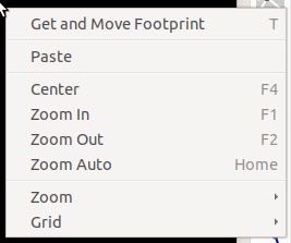
Figure 9.12: Clicking on an empty area of the sheet produces this context menu.
These are functions that allow you to reposition the sheet, zoom in and out, and change the grid size.
Hotkeys in Pcbnew are as important as they are in Eeschema. Most of the hotkeys that you are already familiar with from Eeschema will work in Pcbnew, but there are some differences, so it is worth spending a few minutes here.
With Pcbnew in focus, type '?' Or Alt-F1. You will see the Hotkeys List (Figure 9.13.
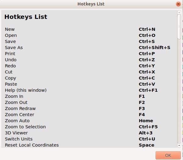
Figure 9.13: The Hotkeys List in Pcbnew.
There are a lot of hotkeys available, but for the purposes of your quick introduction to Pcbnew, only a few are necessary. To use a hotkey, simply place the pointer of your mouse over a footprint, track, text or another part of the layout sheet and type the hotkey.
Hotkey |
Role |
O |
Add a new footprint to the sheet |
E |
Edit, reveals a dialog box where you can edit all footprint attributes |
R |
Rotate (each time you press 'R', the footprint will rotate by 90 degrees) |
G |
Drag, useful for repositioning a footprint without disconnecting any wires. At the time of this writing, the Drag feature is not working as expected; instead it operates as a regular Move. |
M |
Move. If the footprint has tracks connected, the wires will be disconnected |
del |
Delete track or footprint |
C |
Copy item |
X |
Start drawing a track |
V |
Add a via |
T |
Add graphics text, useful for providing information about the schematic |
F3 |
Redraw the sheet, useful when you want to clear graphics artefacts |
Table 9.1: A list of the most frequently used hotkeys in Pcbnew.
There are more hotkeys available in Pcbnew, but the ones listed in Table 9.1 are the most useful ones. Before long, you will commit them to memory and use them constantly.
If you wish to change some of those hotkeys, you can. The process is the same as the one you learned about in the Eeschema segment. Click on the Preferences menu item, then Hotkeys Options, and then Edit Hotkeys (Figure 9.14).
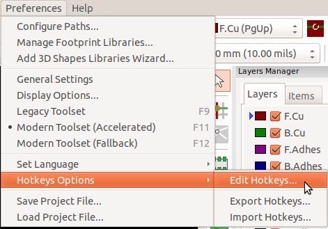
Figure 9.14: How to edit your hotkeys in Pcbnew.
This will reveal the Hotkey editor (Figure 9.15):
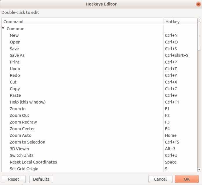
Figure 9.15: Select an existing Hotkey to highlight it, and then type in a new key or key combination.
To change a Hotkey, simply select it with your mouse and type in a new key or key combination.
Now that you know how to use your mouse and keyboard to control Pcbnew, let’s move on to the next topic and learn about the toolbar functions.
Pcbnew toolbars and menus
In Pcbnew, the available functions and tools are grouped in toolbars, menus, and the status bar.
You can see the standard Pcbnew window in Figure 9.3. Following is a quick summary of the purpose of each bar. We’ll look at some more details at later parts of this book.
The left toolbar, marked '2' in Figure 9.3, contains functionality for controlling the visual representation of the various elements of the PCB, as well as of the user interface. For example, you can turn on or off the display of rats nest lines. These lines show incomplete connections between pads. You can also show or hide the part of the right toolbar that allows you to switch to particular layers.
The right toolbar, marked '3' in Figure 9.3, contains the mains functions needed for editing the contents of the sheet. This is where you will find buttons for adding a new footprint, new tracks, and vias, text or graphics on your sheet.
Next to the right toolbar is the Layers manager, marked '4' in Figure 9.3. You can hide it by clicking on the Layers button in the left toolbar if you are working on a small monitor and you want to maximize the available space in the sheet. The Layers manager allows you to select the board layer on which you want to work next. For example, if you want to work on the front layer, you will click on the 'F.cu' option to select it. If you want to work on the back layer, you will click on the 'B.cu' option.
At the top of the Pcbnew window are three groups of functions. Two toolbars, and the drop-down menus. Marked as '5' in Figure 9.3 is the Sizes toolbar. It allows you to select sizes for the tracks, vias and the sheet grid.
On top of it is the main functions toolbar, marked as '6' in Figure 9.3. This is where you will find functions for saving your work to a file, printing your layout on paper, exporting it for manufacturing, performing the design rules check (an equivalent of the Electrical Rules Check in Eeschema), and importing the Neltlist file that you created in Eeschema.
Finally, at the very top of the Pcbnew user interface, we have the drop-down menus. Many of the functions that are available through the toolbar buttons are also available through the menus and, of course, through hotkeys. But there are several functions that are only available through the menus. An example is the Preferences menu, where its contents are only available through it.
Let’s have a closer look at the items that I described above, and learn the most frequently used functions by continuing the work we started in Eeschema. We’ll design a very simple PCB for our resistor and LED circuit.
Left toolbar
In the left toolbar (Figure 9.16) there are several functions there are familiar from Eeschema. For example, buttons labeled 2, 4, 5, and 6 have the same functionality in Pcbnew as they have in Eeschema.

Figure 9.16: The left toolbar.
For now, let’s not be concerned with buttons 1, and 7 to 16. These will make more sense when we are working on a more elaborate PCB so that we can make use of them.
Let’s try out the grid button (2). Click on it to enable it. You should see a thin black box around it, indicating that the grid is enabled. White horizontal and vertical lines should be visible in the sheet if the grid size is of an appropriate size. In Figure 9.17, I have enabled the grid and set its size to 1 mm.
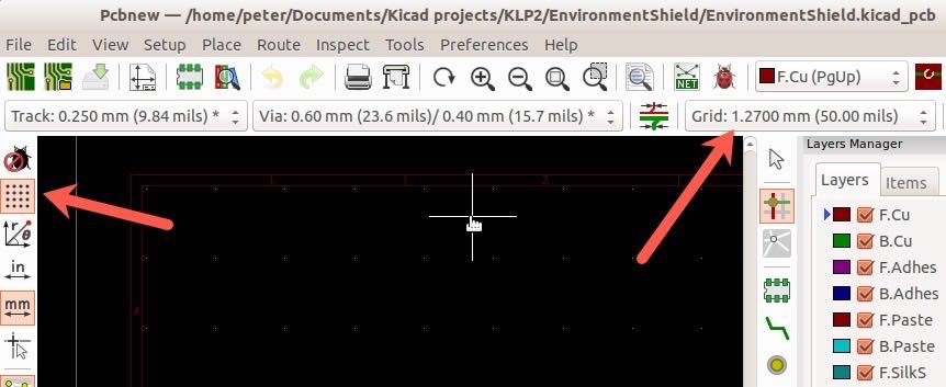
Figure 9.17: Enable the grid and adjust the grid size.
Button 3 allows you to change the relative coordinate system from Cartesian to Polar. I am more accustomed to the Cartesian system so I stay with the default. With the relative coordinate system, you can measure the distance between two locations in the sheet. This is a very useful function in Pcbnew as we want to design very accurate boards that will match well with the components we plan to attach. In Figure 9.18 you can see the Cartesian and Polar coordinate values as they appear in the status bar.
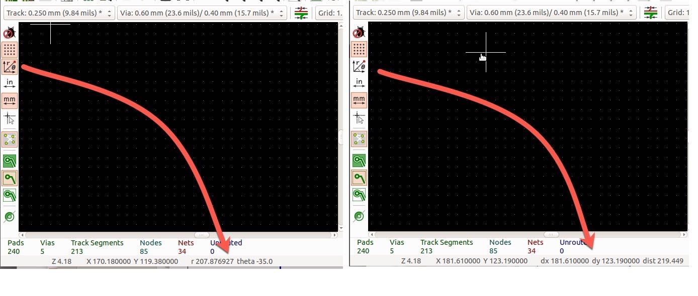
Figure 9.18: Cartesian (right) and Polar (left) coordinates.
Buttons 4 and 5 allow you to switch the length measuring units to millimetres or inches.
Button 6 allows you to change the shape of the cursor to be either a simple pointer or a pointer with crosshairs that reach the sides of the Pcbnew window, as you can see in Figure 9.19.
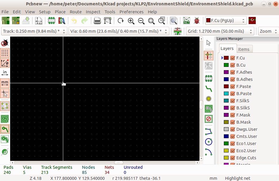
Figure 9.19: Pointer type changed to crosshairs.
In the next segment, we’ll have a look at the top toolbar. You will learn how to use the Netlist button to import the schematic from Eeschema so that you can start working on the layout for your first PCB.
Top toolbar
The top toolbar contains several groups of buttons that include principal functions in Pcbnew. These functions allow you to save the layout to disc, print it to paper or to a format that is supported by PCB manufacturers, select a layer in which to continue work, import a netlist, and more.
In Figure 9.20 you can see an example of the top toolbar.

Figure 9.20: The top toolbar in Pcbnew.
As you can see, there is a lot going on here. Some of the buttons should be familiar to you; you saw them in Eeschema. With reference to the numbers in Figure 9.20, buttons in groups 1, 3 and 4 work the same in Pcbnew as they do in Eeschema.
Let’s explore some of the most commonly used functions of the toolbar by continuing with the simple project we started in the Eeschema segment.
Import the Netlist
The layout work begins by importing the Netlist file. I remind you that this file contains the information that Pcbnew needs in order to import the necessary footprints and setup the ratsnests in the layout sheet. The ratsnests are thin lines that connect the footprint pins that must be electrically connected.
Let’s do this now. Click on the Netlist button, marked '6' in Figure 9.20.
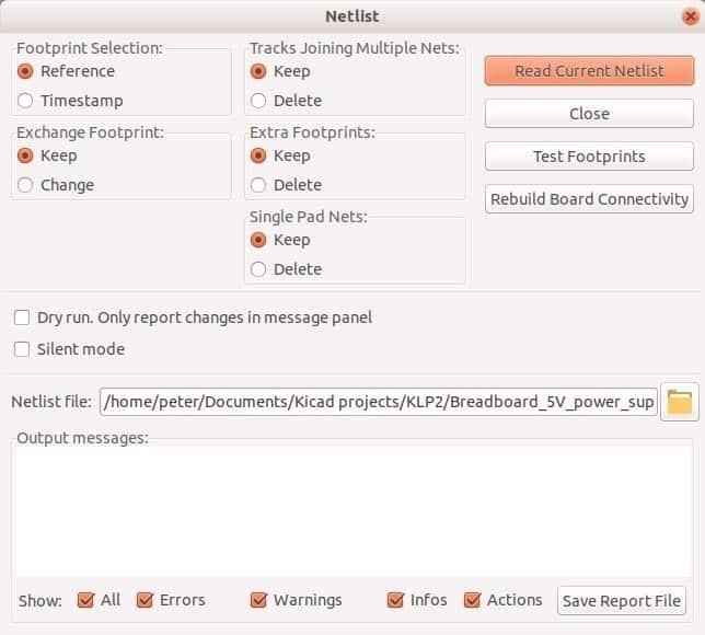
Figure 9.21: The Netlist window.
The Netlist window will appear. There are a lot of options that allow you to fine-tune the behaviour of the Netlist import function. As we are importing a Netlist to an empty sheet, the actual setting don’t matter. However, imagine that you are importing a Netlist to a layout that already has footprints in it. Perhaps you had to go back to Eeschema to make updates and corrections, which resulted in a new Netlist file. How would you like Pcbnew to handle components that have a new footprint? Or a footprint that exists in the sheet but not in the Netlist you are about to import? These are things we can control by making appropriate choices in the Netlist window.
In this example, we will accept the default options and let the import proceed. Notice that in the 'Netlist File', the Netlist file we created in Eeschema is already listed. If it isn’t, click on the Browse button to find it and select it.
Next, click on the 'Read Current Netlist' button. Pcbnew will read the file and show you the results in the Messages text area. The window will not disappear. Move it a little to the side, and notice that the circuit’s footprints are now in the layout sheet.
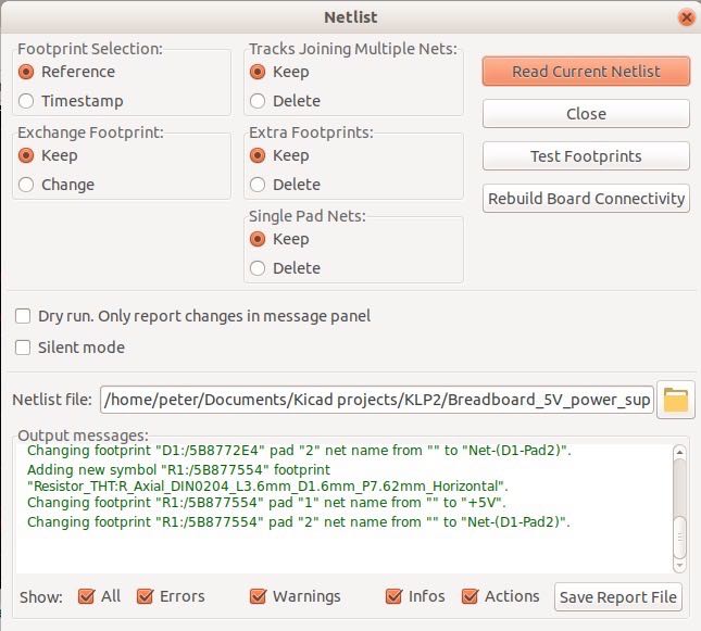
Figure 9.22: Reading the Netlist file will place the footprints to the sheet.
Click on the 'Close' button to dismiss the window. Let’s concentrate on the footprints that we just added to the layout sheet.
Move footprints
The two footprints should be attached to your mouse pointer. Click anywhere inside the sheet to place them.
Place your cursor on the footprint bundle and use the scroll wheel to zoom in.
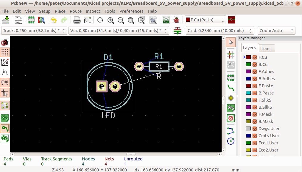
Figure 9.23: Zoom into the footprint bundle.
Let’s separate the footprints manually. Use the 'M' hotkey to move one of the footprints away from the other. When footprints and other items are overlapping, the exact location where you mouse course is at may be occupied by more than one of them. When that happens, Pcbnew does not know which item you want to operate on. It will produce a context menu asking you to clarify.
It looks like in the example in Figure 9.24, where I placed the mouse pointer on a location where three items 'exist', a pad, and the two footprints. Then, I typed 'M', for 'Move'. I am working at zoom level 7.33 and grid size 0.25 mm.
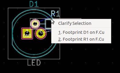
Figure 9.24: A context menu asking for clarification of item selection.
You can click and select one of the footprints. This will attach the footprint to your mouse pointer. You can then move it, and do a left-click to place the footprints on its new position.
Alternatively, because the LED footprint is larger than the resistor, it is an easier target. Place your cursor on it, taking care to be clear of the resistor, and again type 'M'. In Figure 9.25, you can see how I moved the LED footprint to the left of the resistor.
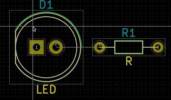
Figure 9.25: The two footprints are not overlapping.
Let’s rotate the resistor by 90 degrees. Place your mouse pointer over the resistor footprint, and type 'R', for 'Rotate'. You will also need to use 'M' on the resistor to move it a bit to the right, as in the example in Figure 9.26.
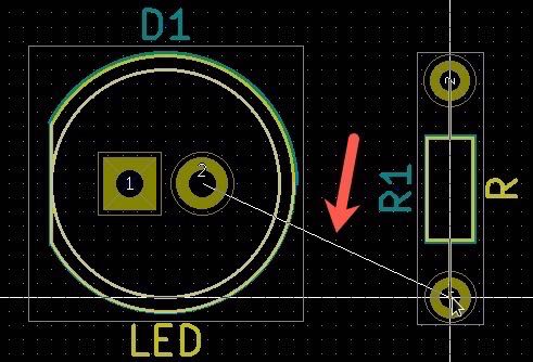
Figure 9.26: Move the resistor by 90 degrees. The arrow shows the ratsnest line.
In Figure 9.26 you can also see the single rattiest line, which indicates that we must create a track that connects pad 2 of the LED footprint (D1) with pad 1 of the resistor footprint (R1).
Design Rules Check (DRC)
At the moment, we have the two footprints in the sheet, placed at locations where I think are appropriate for this project. We will need to use some of the tools in the right toolbar, but before we get to it, I’d like to introduce a few more of the functions from the top toolbar.
One of the most important functions is the Design Rules Check (DRC) which you can access via the button labeled '7' in Figure 9.20. The DRC is similar to the ERC in Eeschema. It checks your layout for errors.
The most common errors that the DRC can find are things like:
- two tracks are too close to each other
- no tracks connecting pads that should be connected
- a track is too close to a pad
- a track is to close to the edge of the board
- a track is too close to a via
- a via is too close to a pad
There are more, of course. The details of things such as 'when are two tracks too close to each other' and ' when is a track too close to a pad', are all configurable by editing the Design Rules for the project. You can do that by calling the Design Rules Editor from the Pcbnew main menu item 'Setup' (item '7' in 9.3). The Design Rules Editor looks like the example in Figure 9.27.
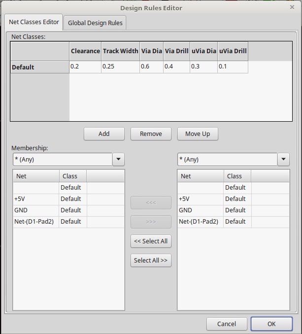
Figure 9.27: The Design Rules Editor in Pcbnew.
In Figure 9.27 you can see the default design rules. All the values are in millimeters. As per these rules, tracks must be 0.2mm away from other tracks, vias, and pads, or more. The width of a track must be 0.25mm or more, and so on. You can also see the default global design rules by clicking on the 'Global Design Rules' tab. For the purposes of this simple project, we will work with these default rules. In later projects, you will learn how to make modifications to the design rules. Let’s click on the 'Cancel' button to exit this dialog box.
Next, let’s do a DRC now, even though we know that our layout is not complete. I’d like you to see what a DRC error looks like, and learn to interpret it. Click on the DRC button, and the window depicted in Figure 9.28 should appear.
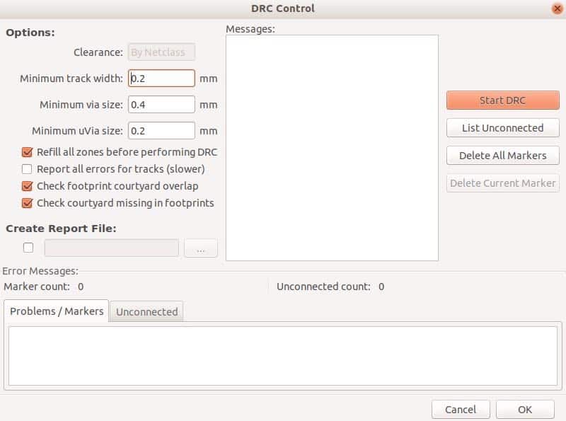
Figure 9.28: The DRC Control window.
On the left side of the DRC Control window, notice that there are several options, such as 'Min track width' and 'Min via size'. These values are copied from the Global Design Rules settings. You can confirm that by clicking on the 'Global Design Rules' tab in the Design Rules Editor (Figure 9.27). The DRC Control window allows you to change these values to you can try the DRC with custom values.
For example, let’s say that the default values case the DRC to report an error because a track to closer than 0.2mm to a pad. If you know that your PCB manufacturer can accommodate clearances of 0.1mm, then you can use '0.1' as a custom value in DRC Control to see if the error still comes up. If not, then you can continue with your work, knowing that your manufacturer will be able to produce the board. But if the error comes up again, you will know that you have to move the track further away from the pad.
To start the check, click on the 'Start DRC' button. The result should be what you see in Figure 9.29.
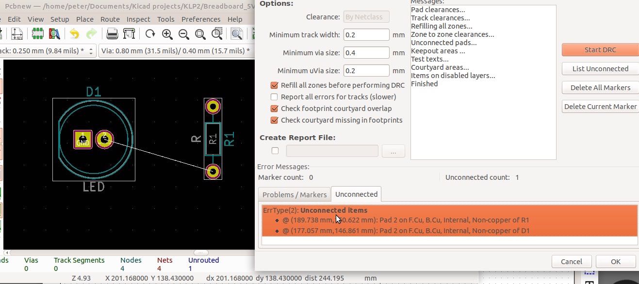
Figure 9.29: The DRC reveals that two pads are not connected.
The DRC reveals no problems in the Problems/Markers tab, but show two unconnected pads in the Unconnected tab. If you click on the error message, it will automatically zoom and pan into the location of the error. This error is easy to understand: Pad 1 of the R1 footprint on the front copper layer, which also exists in the back copper layer (since this is a through-hole component), should be connected to Pad 2 of the D1 footprint.
Let’s fix this. We will need to use the Wire tool that belongs to the right toolbar. In Figure 9.30, the arrow points to the Wire tool. You can also activate the Wire tool by typing the 'X' hotkey, which is how I prefer to do it.
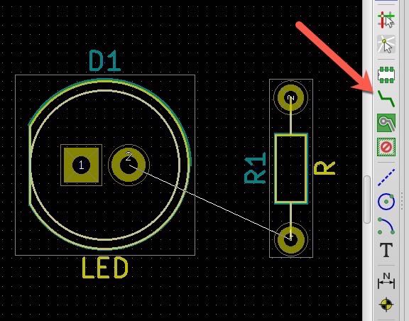
Figure 9.30: The Wire tool.
Place your mouse pointer over pad 1 of the resistor, and then type 'X'. With the wire tool selected, mouse your mouse slightly to the left, and notice that a thick red line that connects pad 1 of the resistor with the mouse cursor (Figure 9.31).
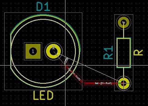
Figure 9.31: Drawing a new track.
As you are drawing the track, notice that the ratsnest line that connects pads 1 and 2 is still showing. This indicates that the electrical connection is not complete. Place your cursor in the middle of pad 2 of D1, and double click to complete the new track.
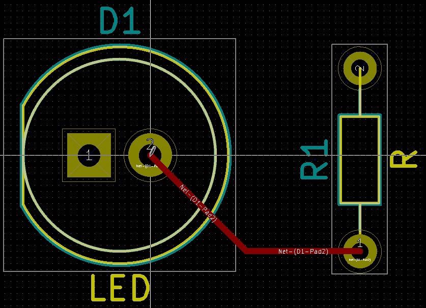
Figure 9.32: Completed drawing a new track.
You now have a completed electrical connection between the two pads, and the ratsnest line has disappeared. A solid red line with two segments represents the new track. When you manufacture this board, this red line will be implemented with copper.
The line of the track is important. By default, red refers to the top copper layer, and green refers to the bottom copper layer. You can see which colours represent the various PCB layers by inspecting the 'Visibles' panel on the right side of the Pcbnew window. Figure 9.33 shows the first few items in the list, which includes the top and bottom copper layers.
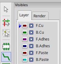
Figure 9.33: Each layer has its own colour.
With the only unconnected pair of pads connected, there should be no more DRC errors. Repeat the DRC to make sure. It should come back clean, with no errors in the Problems/Markers and Unconnected tabs.
There is still more work to be done. At the very least, we must add a connector so that we can connect this simple circuit to a battery. We also need to mark the borders of the PCB so that Pcbnew, and eventually the manufacturer, know where to cut the board. But before we get to that, let’s have a look at the 3-D representation of our work so far. In the main menu, click on View, and then click on '3D Viewer' (Figure 9.34).
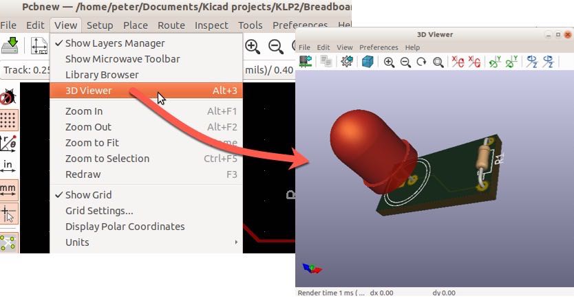
Figure 9.34: a 3-D representation of our incomplete board.
In the 3D viewer, you can manipulate the model using your mouse. Zoom in and out, pan and rotate. You can get a very accurate preview of what the PCB will look like if you went ahead to manufacture it. Many footprints, like the LED and the resistor, have 3D models that are used to render this view. If a footprint does not have a 3D model, only its pads will be shown.
Plot for Gerbers
While we are still on the top toolbar, let’s have a quick look at the Gerber plotter and the layer chooser. You can access the Gerber plotter by clicking on the button with the plotter icon in the group of buttons marked '4' in Figure 9.20. In Figure 9.35 you can see the Plot window.
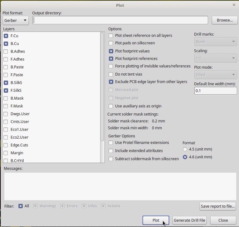
Figure 9.35: The Plot window from where you create the Gerber files.
When your layout work is complete and you are ready to send it to a manufacturer, you will need to create several files that contain the necessary board information. The Plot window is where this operation takes place. Several files are needed because a PCB is the combination of multiple layers and holes. You already know about the top and bottom copper layers, but there are more. For example, there is the layer on which the graphics are printed, both on the top (front silkscreen, or 'F.Silk') and the back (back silkscreen, or 'B.Silk'). There is also the solder mask, front, and back ('F.Mask' and 'B.Mask' respectively). The solder mask is a polymer material that is applied over the copper traces to prevent short circuits and protect against oxidisation. It also makes it easier to solder components onto the board by preventing the solder from spreading away from the pads and onto the tracks.
Each of the layers that your PCB uses is described by its own file. In the Plot window, you will select which files you’d like to create and then click on the Plot button to have them created.
Most PCBs also have holes, used to implement things like vias, pads for through-hole components, and opening for mounting screws. There is a separate file that you must create that will contains information about these holes, called the 'Drill File'. To create the Drill File, click on the 'Generate Drill File' button, which is right next to the Plot button. This will bring up the Drill Files Generation window, that you can see in Figure 9.36.
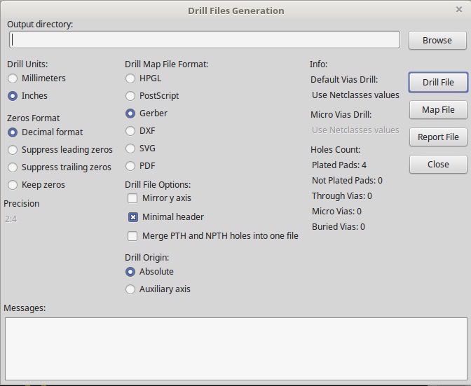
Figure 9.36: The Drill Files Generation window from where you create the Drill File.
Pcbnew can explore files in several different formats, but every manufacturer I have ever used can work with Gerber-formatted files, so we will use this type in this book. By default, Gerber is selected for the Drill Files and the Plot files.
The exact options that you should select depend on the expectations of your PCB manufacturer. For example, OSHPark has a guide to help you with the Gerber export step. OSHPark also allows you to submit the Pcbnew file with the .KiCad_pcb extension, and avoid having to create the Gerber files altogether, which is a welcome convenience. Pcbway.com also has a guide that details the Gerber file export process from KiCad.
I will show you how to do both in the next project, in which we will design and produce a PCB.
Layer chooser
The last top-menu item that I’d like to introduce is the Layer Chooser. It is labeled '8' in 9.20. You can see it extended in Figure 9.37.
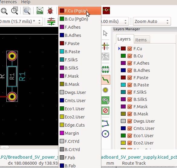
Figure 9.37: The top-menu dropdown allows you to switch between layers.
The Layer chooser in the top toolbar contains the exact same items as the Layer tab in the Visible pane next to the right toolbar. It allows you to switch between layers.
Let’s do a quick experiment. Let’s delete the only track so far, and redraw it, but this time in the bottom layer.
First, the delete part. Place your mouse cursor over the red track. Try to avoid any areas where the track overlaps something else, like a pad. If you do, Pcbnew will ask you to clarify your selection with the context menus you saw previously. With your mouse over the track, hit the 'delete' key on your keyboard. The track will disappear, and the ratsnest will appear in its place.
Next, click on the Layer Chooser to open it, and click on B.Cu (Back Copper) to select it. Notice the small triangle pointing to 'B.Cu' in the Layer tab of the Visibles pane (Figure 9.38).
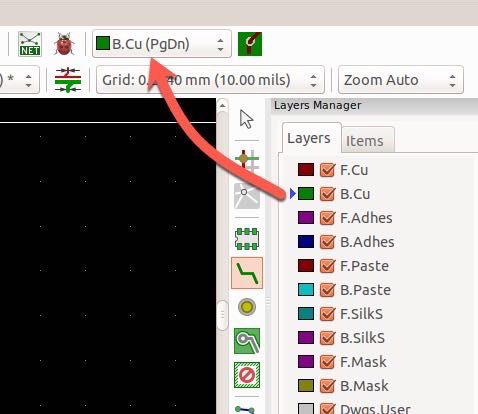
Figure 9.38: The back copper layer is selected.
Now, let's re-draw the track. Place your mouse over one of the pads indicated by the ratsnest, and type 'X' to start drawing. Complete the drawing by double left-clicking on the other pad. Your layout should look like the example in Figure 9.39. The track is now green instead of red since it is in the bottom copper layer.
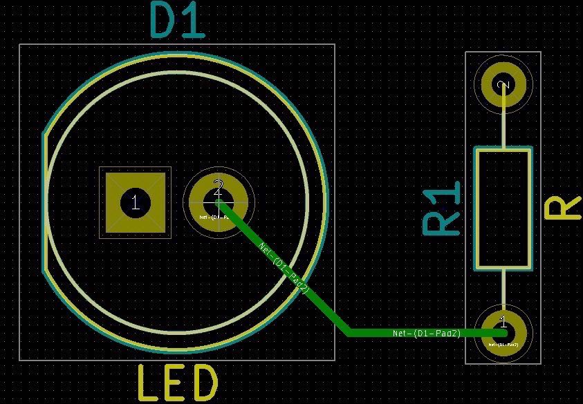
Figure 9.39: A new track in the back copper layer.
With two-layer boards, it does not matter much whether a track is placed on the top or the bottom layers. These days, single and double layer boards bring no material differences in cost or manufacturing processes.
We will discuss PCB design principles and considerations later, and learn good common practices for choosing positions for footprints and tracks, but for now let’s continue to focus on Pcbnew.
Right toolbar
The right toolbar is where you will find the various drawing tools. With these tools, you can add and remove footprints, graphics, text, dimensions and, of course, tracks to the layout sheet. In Figure 9.40 you can see the right toolbar annotated with numbers to make reference easier.

Figure 9.40: The right toolbar.
Standard mode
The button, marked as '1' in Figure 9.40, allows you to the standard drawing mode. Most likely, you will enter the standard mode by hitting the ESC key. In Standard mode, you can click and select footprints and other items, right-click to reveal the context menu and measure distances between two points in the sheet.
Try this now: Hit the ESC key to enter standard mode, and click on the LED footprint. You will see that the footprints properties appear in the status bar, at the bottom of the Pcbnew window.
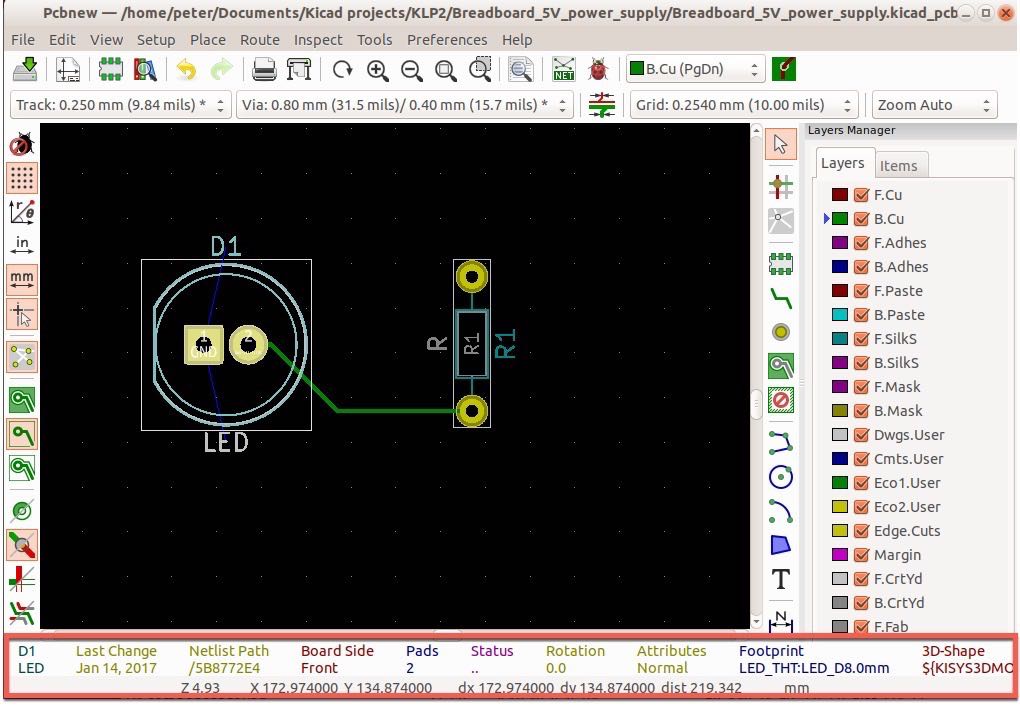
Figure 9.41: Click on an item while in the standard mode to display the item's properties.
In Figure 9.41, I have clicked on the LED footprint. In the status bar, I can see that this footprint designator is 'D1', it is on the front copper layer ('F.Cu'), it has two pads, and more.
Try clicking on the green track, that connects the LED to the resistor. The status bar will tell you that the name of the net which is implemented by the track is 'Net-(D1-Pad2)', and that it is drawn in the back copper layer ('B.Cu').
Net highlighter
The next button in the right toolbar, marked '2', is the net highlighter. While our current PCB is minimal, with a single net[5], you will quickly find yourself working on PCBs with many nets. In Figure 9.42 you can see an example PCB that contains several more nets than our current PCB does.
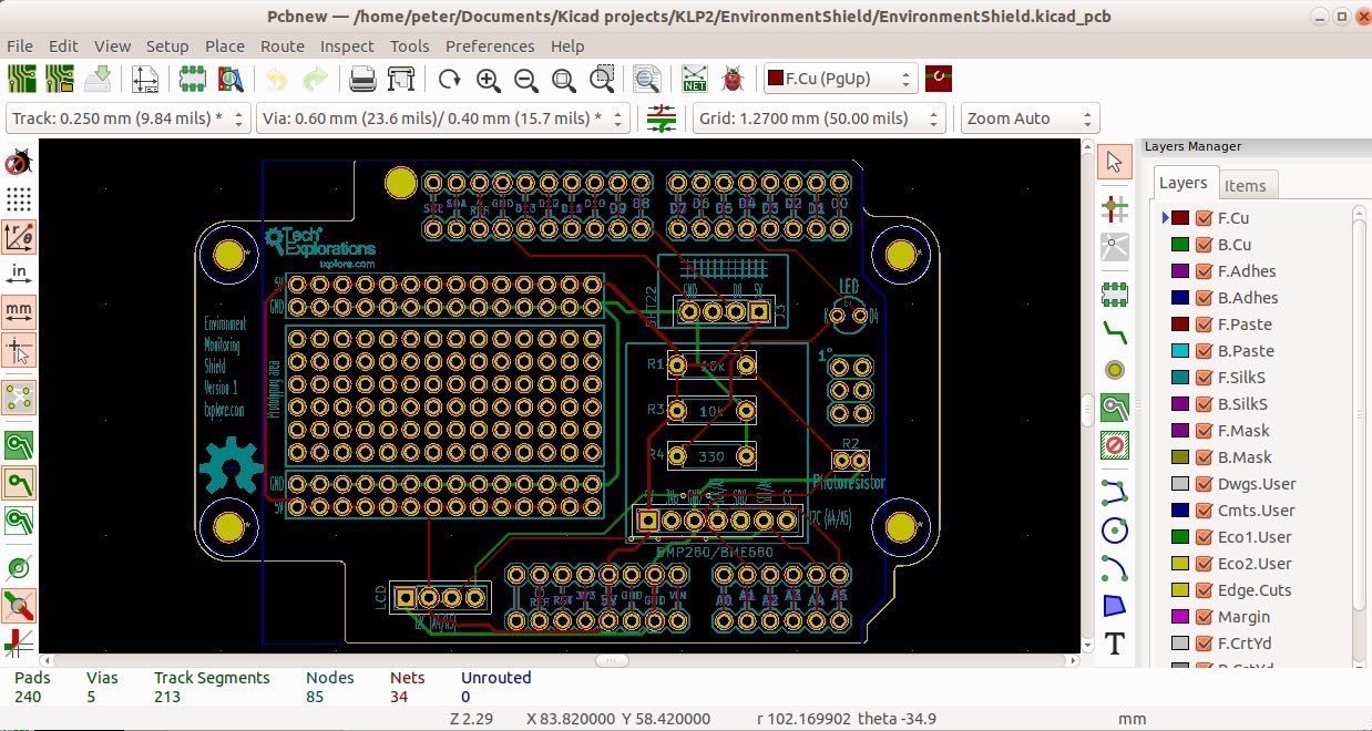
Figure 9.42: A PCB with several nets.
With only a glance at this board, it is hard to determine which tracks belong to, say, the 5V track or the GND track. But with the help of the Net Highlighter tool, this task becomes much easier. Click on the Net Highlighter button.
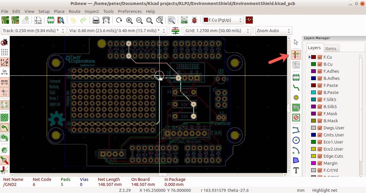
Figure 9.43: The Net Highlighter makes it easy to see tracks among other tracks.
In Figure 9.43 you can see the highlighted green track, with the net name 'GND2’ running from the bottom left of the image to around the middle right side. Notice that the Net Highlighter tool is enabled.
Add footprint
When you imported the Netlist file into Pcbnew, Pcbnew automatically added the specified footprints into the sheet. If you want to add additional footprints, you can do so using the Add Footprint button, marked as '4' in Figure 9.40.
In our simple PCB, there is currently no provision for an external power source that will provide the power needed to light up the LED. It would be good to be able to add a simple connector for this purpose.
Let’s go ahead and do this now.
First, you need to decide what kind of connector to add to your board. You can choose between something very simple, like two large pads on which you can solder the power source wires. You can also choose a barrel connector plug, a header connector like the ones used on the Arduino, or a screw terminal. Of course, there are many more options.
Let’s assume that you have chosen a screw terminal, like the one in Figure 9.44 for the convenience of being able to securely attach the wires that come from a small AA battery pack.
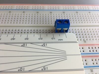
Figure 9.44: We’ll add this screw terminal to our project layout.
To add a new footprint, click on the Add Footprint button, or type the 'O' hotkey. If you use the hotkey, first place your cursor on the approximate location where you would like to attach the new footprint. The Load Footprint dialog box will appear, as in Figure 9.45.
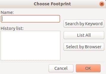
Figure 9.45: The Load Footprint dialog box.
This is not very useful. We don’t know or remember the name of the screw terminal footprint, and the history list is empty. The easiest way to find a footprint when you don’t know exactly what you are looking for is to use the footprint browser.
Click on the button marked 'Select by Browser' to reveal the footprint browser window (Figure 9.46).
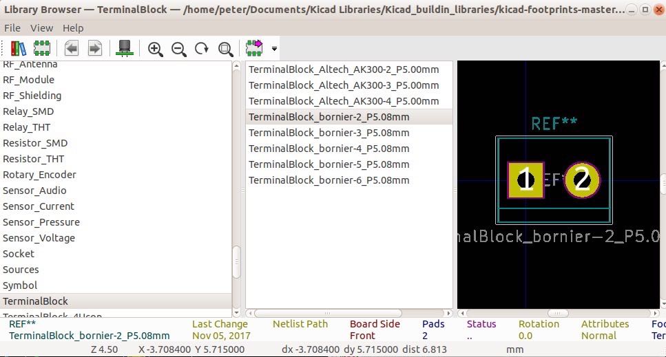
Figure 9.46: The footprint browser.
The footprint browser contains three panes. The one in the left lists the available libraries; the one in the middle lists the footprints that belong to the selected library; and the one in the right shows a visual representation of the selected footprint. Take some time to browse around the various libraries and footprints.
The footprint browser also gives you access to the 3D viewer. The 3D viewer gives you a 3D rendering of what the selected footprint looks like on a 'virtual' PCB. To use it, click on the button with the integrated circuit icon, as in the example of Figure 9.47.
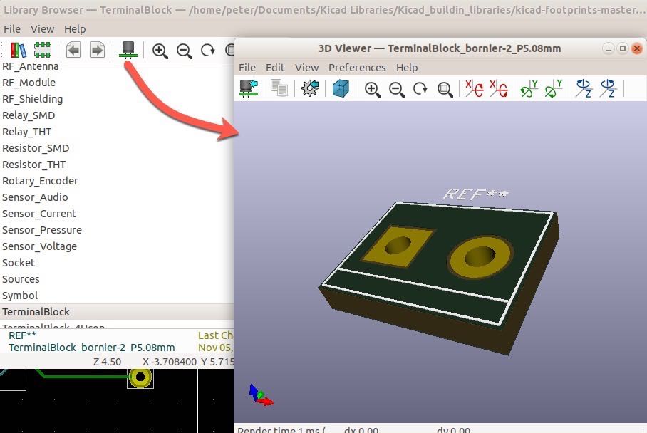
Figure 9.47: The footprint browser.
A good candidate for the 2-pole screw terminal we are looking for is inside the Terminal_Blocks library. There are several footprints in this library, and we want the one with the 2 pads, and 5.08 mm distance between the centres of the pads. The distance between the pads is conveniently provided as part of the name of the footprint, but that is not always the case. I have cultivated the habit of measuring a footprint to confirm it will match the real-world part before I drop it to the layout sheet.
First, notice that in Figure 9.44, the rules against the pins of the screw terminal shows that the distance between them is a bit over 5.08 mm. If you want high accuracy, you can use a calliper to make these measurements (this is something I will show you how to do in a later project). Another thing you can do is to measure the pin distance against a length that you already know is correct. In this case, You can plug the screw terminal into a standard breadboard that we know has a socket pitch of 2.54 mm. The screw terminal pins span across three breadboard holes, so the total distance is 2.54 x 2 = 5.08 mm.
Let’s go back in the footprint browser. Remember in Eeschema that we can use the distance counter to measure the distance between to locations of the sheet? We can use the exact same function in most apps in KiCad. Let’s use it to confirm we have the right footprint. Place your mouse cursor in the middle of pad number 1, and press the space bar to zero the dx and dy counters. Then move your cursor to the middle of pad number 2. Look at the dx reading in the status bar. It should show 5.08 mm (Figure 9.48).
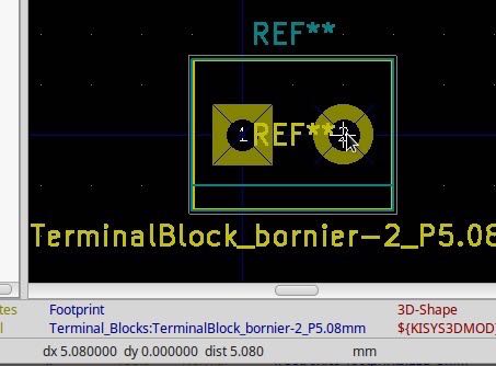
Figure 9.48: The distance between the pads is 5.08 mm.
This is the confirmation we need to be sure that this is the correct footprint for the screw terminal. Double-click on the footprint name to accept it and drop it to the layout sheet (Figure 9.49).
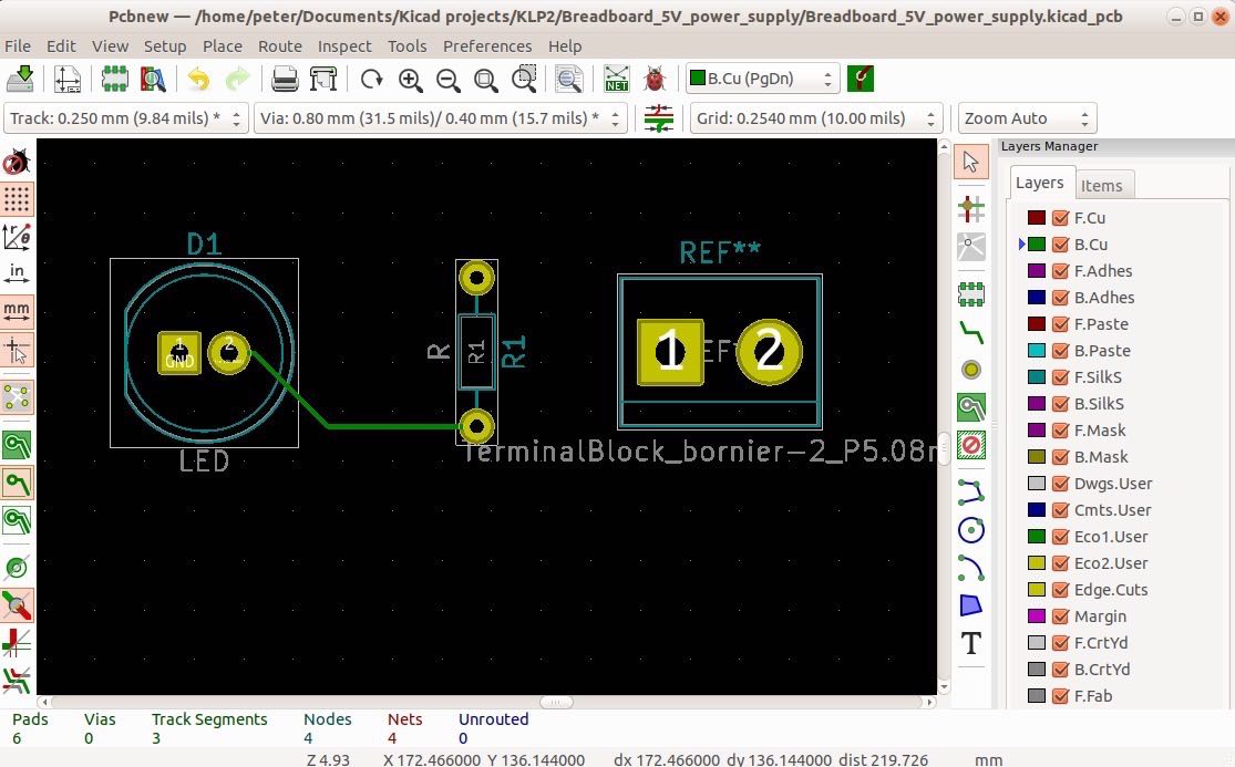
Figure 9.49: The screw terminal footprint is added to the layout.
Before we do the wiring, we should move it to a better position and orientation. Place your mouse cursor over the screw terminal footprint and use the 'M' and 'R' hotkeys to move and rotate the footprint. My version of the layout looks like the one in Figure 9.50.
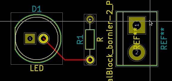
Figure 9.50: The screw terminal footprint at its final position.
With the new footprint in the layout, the next thing to do is the wiring. Let’s do that next.
Wiring
Right below the 'Add footprint' button in the right toolbar is the 'Add tracks and vias' button. We use this button to create, you guessed it, tracks and vias. As always, there are hotkeys to quickly enable these functions: 'X' to add new track, and 'V' to add new vias.
Let’s work on adding new tracks. We need a new track that connects the cathode of the LED to one of the pads of the screw terminal, and another to connect the free pad of the resistor to the other pad of the screw terminal
First, ensure that the front copper layer is selected. We are working on this project as a single-layer project.
Next, place your mouse cursor over pad 1 of the LED, and press 'X' to get into track mode. The tool will start drawing immediate. As you move the mouse, you will see the track being laid behind it. If you make a mistake, just hit the ESC key to cancel out of the track tool, and try again (press 'X' to begin drawing again).
Try to draw the track that starts from the LED cathode pad to pad 1 of the screw terminal. Remember that to end the drawing of a track, double-click. In Figure 9.51, you can see the start of my attempt.
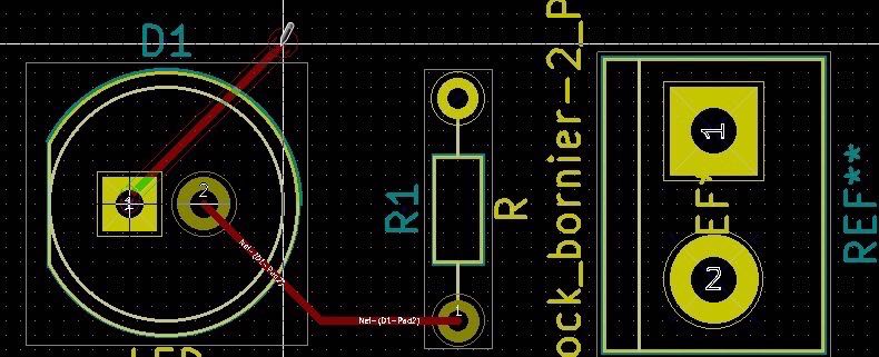
Figure 9.51: A question mark appear as I am trying to draw an ad-hock track.
When you try to end the track by double-clicking, you will notice that Pcbnew is not allowing you to do so. This is because as you are drawing the new track, Pcbnew is automatically checking for violations of the design rules. Because we are trying to create a track that does not exist as a ratsnest, to a footprint that is not in our Eeschema (and Netlist) sheet, Pcbnew assumes that we are doing something illegal.
It is true that a better way to add the screw terminal footprint to our PCB would be to first add it in the schematic diagram (Eeschema), and then import it into Pcbnew through the Netlist, as we did with the other two components. But while that is the orthodox way of doing things, KiCad allows us to work in a more ad-hoc day by turning off the design rules checking. I rarely work this way, but in some cases, this is necessary, as you will see in a more appropriate example later.
To turn off the design rules checking by clicking on the top button in the left toolbar (Figure 9.52).
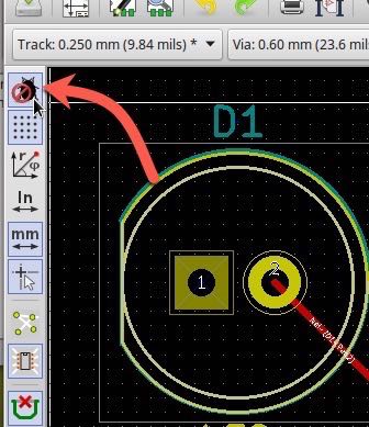
Figure 9.52: Turn off design rules checking.
With the rules checking off, you can draw the new track as you wish. To work with rules checking turned off under KiCad 5 and newer, you will also need to switch to the Legacy Toolset. To do that, click on Preferences and then Legacy Toolset (Figure 9.53).
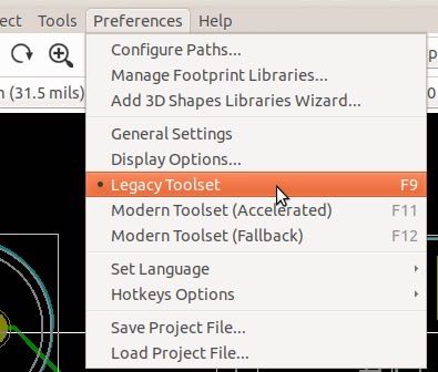
Figure 9.53: To turn off rules checking you must enable the legacy tool set in KiCad 5 or newer.
Place your mouse over Pad 1 of the LED and type 'X'. Do single clicks to create segments, and double-click to finish drawing over Pad 1 of the screw terminal footprint. Notice the '?' at the end of my incomplete track in Figure 9.54? This is a reminder that you are working with design rules checking turned off.
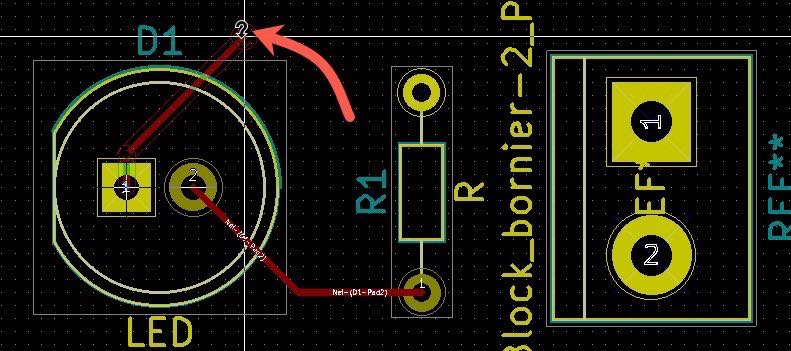
Figure 9.54: The '?' at the end of the track reminds you that you are working with design rules checking off.
Complete the wiring for the two ad-hock tracks, so that the PCB looks like the one in Figure 9.55. The two new tracks complete the circuit. Remember to turn back on the design rules checking.

Figure 9.55: Ad-hock tracks added.
I must repeat that adding ad-hock wires and footprints is not best practice and should only be used for a good reason. It is best to include all components and nets in the schematic diagram, and then bring this information over to Pcbnew where you can do the layout under the supervision of the design rules checker. In this example, however, I wanted to show you the flexibility of KiCad to work without any restrictions, while acknowledging that restrictions are in place for a very good reason: to avoid human errors.
We are close to finishing this first PCB. The few remaining on our to-do list are adding the board cut-out (that defines the borders of the board) and the graphics (things like lines and text). But before we do that, let’s have a quick look at fill zones and keep-out areas.
Fill zones and keepout areas
Buttons marked '6' and '7' in the right toolbar (Figure 9.40) allow you to create copper fill zones and keep-out areas respectively. We will not be using any of the two in this example, but will we in later projects. For now, I’d like you to be familiar with these functions at a high level.
A copper fill is an area on the PCB from where the copper has been left intact, instead of being etched out. In Figure 9.56 you can see an example of copper filled areas in the back of this Arduino Uno clone.
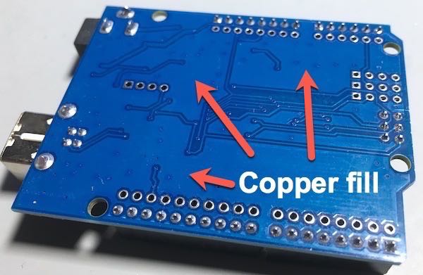
Figure 9.56: The back of this Arduino Uno contains several copper filled areas.
Copper fills (also known as 'copper pours') are commonly used to create a ground plane (as well as 5 V or 3.3 V planes) as a better way to distribute the ground level around the board (as opposed to using traces). Another reason for including copper planes is to reduce the amount of etching chemical needed to remove copper from the raw board[6] and to improve the electrical and radio interference characteristics of the final PCB.
There are different types of copper fills. Most designers tend to opt for a solid copper pour, like the one you see in Figure 9.56. It is also possible to create copper fills that include a pattern of a lattice, like the one in Figure 9.57.
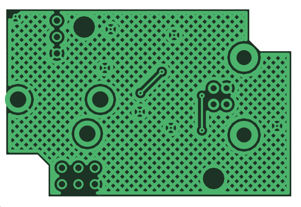
Figure 9.57: PCB board showing copper pour with a hatch fill (Image reused under Creative Commons License, https://commons.wikimedia.org/wiki/File:PCB_copper_pour_hatch_filled.png).
A keep-out area is a part of the PCB where you wish to keep empty of tracks, vias and copper pours. When you create a keep-out area, you can specify which of the above you would like to keep out of it. Your choice becomes part of the design rules checks, and the checker prevents you from adding any of those items in the keep-out area.
You may want to create a keep-out area for things such as having an area that provides structural support for other parts of a gadget, areas that can be snapped off to help in manufacturing, to name a few.
In our current simple design, we will not create a copper fill or keep-out areas, but we will in our later projects.
Edge cut
At the very least, the manufacturer needs to know the shape and dimensions of the PCB, as well as the tracks, holes, and vias on it. So far in this part of the book, we have been working on the tracks and holes for the pads, but not on the PCB’s shape and dimensions. We also haven’t added any graphical design elements, like text descriptions, to be printed on the PCB. Graphics are useful because they both make our PCB more aesthetically pleasing, and because they make the PCB easier to use.
Let’s start with defining the shape and dimensions of our PCB first. This is something that many designers do at the start of the layout process in Pcbnew, instead of the end as we are doing here. The advantage of doing it at the start is that we can set the physical constraints of our PCB early on. Imagine that you want to design a PCB that fits nicely inside a project box. This is a major constraint, so you should set it in your design before you start placing footprints and tracks on it. If you leave it for the end of the process, you may find that the footprints and tracks are placed in a way that makes the PCB bigger than the box. This will require a lot of rework so that everything fits.
To draw the border of the PCB, first, select the Edge.Cuts layer from the layers manager toolbar or drop-down (Figure 9.58). The Edge.Cuts layer is a special layer that contains information that the manufacturer needs in order to know where to cut the board. When you export the Gerber files, the Edge.Cuts layer information is exported into its own file.
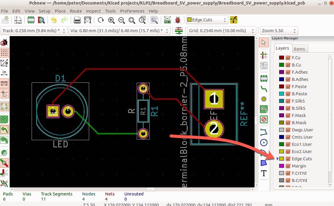
Figure 9.58: To create the PCB perimeter, select the Edge.Cuts layer first.
With the Edge.Cuts layer selected, you can use one of the graphics tools marked as '8' in Figure 9.40 to draw it. Using the line, arc, and circle tools you can create elaborate shapes for your PCB. Let’s start with something simple: a rectangular PCB. Once we have this simple design ready, we can retrofit it easily by adding space for two mounting holes along the two ends of the rectangle.
Click on the line tool and start drawing the perimeter. As you are drawing the perimeter, keep in mind that the polygon you produce must be contiguous. That is, there must be no breaks anywhere along the polygon that makes up the perimeter. A common problem here is that the start of the line with the end does not meet precisely. Close the polygon so that your PCB now looks like the example in Figure 9.59.
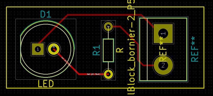
Figure 9.59: The perimeter of the PCB is a simple polygon.
Look at the 3D representation of your board by clicking on View and 3D Viewer. It should look like the example in Figure 9.60.
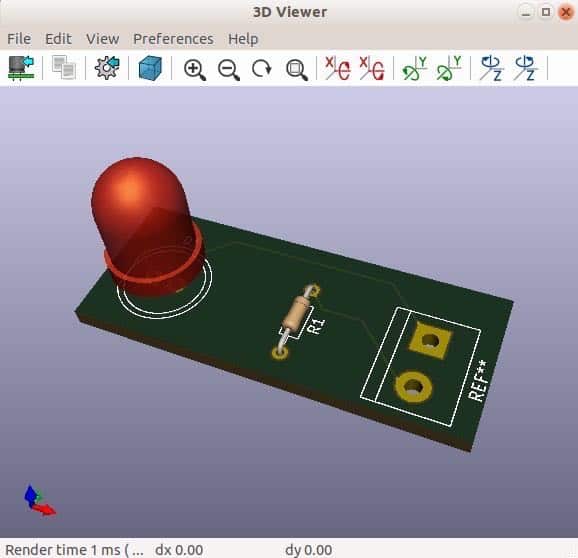
Figure 9.60: The 3D representation of the rectangular PCB.
Let’s add another feature to this board, a mounting hole. With a mounting hole, you can secure your PCB to an enclosure with a screw. The easiest way to add mounting holes to your PCB is to add a single pad and modify it’s drill size to accommodate the size of the screw.
First, think about the screw you’d like to use. In my case, I’d like to use a nylon screw, with a width of 2.97 mm, as measured with my calliper (Figure 9.61).
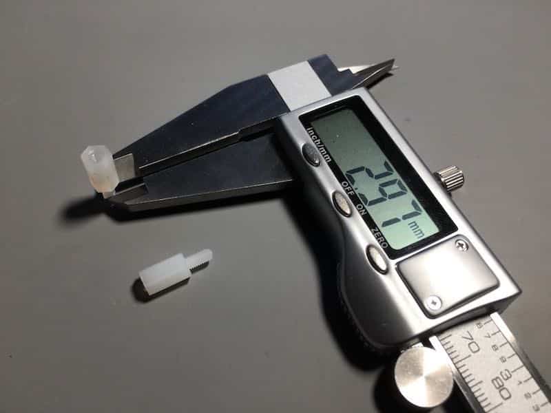
Figure 9.61: Measuring sizes with a calliper is easy and accurate.
We will need an opening slightly larger than 2.97 mm on the board. When you consider adding mounting provisions to your PCB, you should think about where the PCB will be eventually installed. It could be placed inside a project box, or stacked onto another PCB, or perhaps used on a breadboard. In the case of our example, let’s plan to have it mounted on a plastic surface, using two screws. We can place the screws along the X or Y axis of the board. I’ll go for the X-axis. I’ll place one screw hole on the left of the LED, and another on the right of the screw terminal.
Let’s add the first opening. Place your cursor on the right side of the LED, as I show in Figure 9.62, and type 'O' to add a new footprint. Do a right click to bring up the Load Footprint dialog box, and then click on 'Select by Browser'.
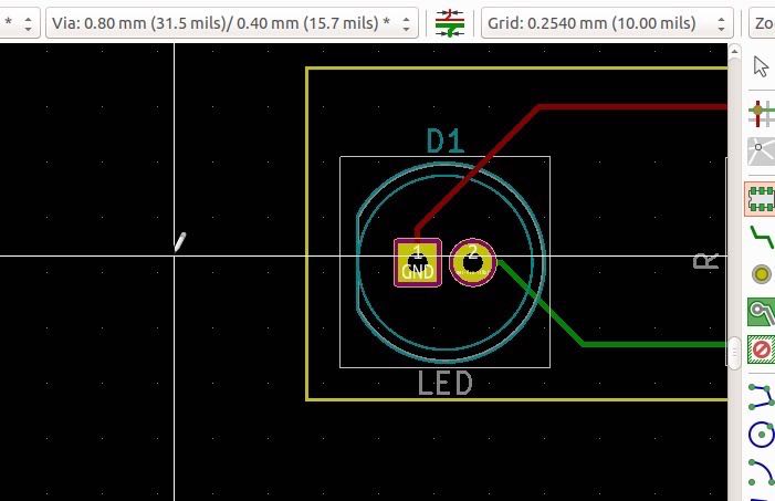
Figure 9.62: We’ll place the new screw opening at the approximate location of the cursor.
In the Library Browser windows, look for the 'MountingHole' library in the left pane, and select the 2.7mm hole footprint (Figure 9.63).
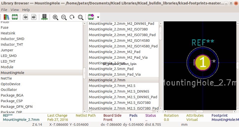
Figure 9.63: 1 pin footprints make good screw holes.
Double-click on the 2.7mm item to select it and drop it to the layout sheet. Position it close to the LED, as in the example of Figure 9.64.
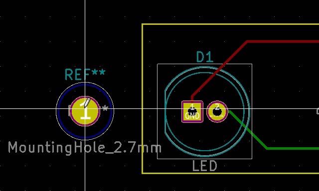
Figure 9.64: The first screw hole is placed.
We’ll add a second screw hole next to the screw terminal, but first, we have to confirm that the one we just added has the correct drill size. Place your mouse pointer over the 1pin footprint, and type 'E' (for 'Edit'). Be careful where you place your mouse pointer because its position dictates the properties window that will appear. For example, if you place your mouse over the blue circle in the outer region of the footprint, you will get a properties window that belongs to the back or front paste layer. We want the properties of the hole, so make sure to place your mouse pointer right in the middle of the footprint, as I show in Figure 9.64.
You can see the screw hole properties window in Figure 9.65.
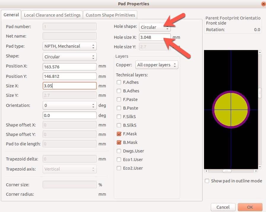
Figure 9.65: properties for the screw hole.
The arrows in Figure 9.65 show the properties that are most relevant to what we are trying to do here: the shape and size of the drill. We want a circular hole (not oval), so the default shape is good. We want a drill size that is slightly larger than the diameter of the nylon screw I am planning to use (which I measured at 2.97 mm). At 3.048 mm, the drill size is also good. With this information, we know that the screw opening is appropriate. Click Ok to close the properties window.
Let’s duplicate this hole so that we can add an identical one next to the screw terminal. Place your mouse pointer over the yellow circle at the perimeter of the hole, and type Ctrl-D to duplicate the footprint (Figure 9.66).
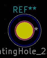
Figure 9.66: When duplicating a footprint using Ctrl-D, take care to place the mouse pointer on the yellow line.
Using Ctrl-D can be tedious because the correct target is a very thin line. You can zoom in to increase the size of the target, or you can use the context menu. To use the context menu, place your mouse point right in the middle of the footprint and left-click. You can then follow the context menu by selecting the footprint name and then 'Duplicate Footprint'.
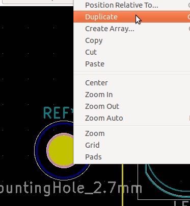
Figure 9.67: You can duplicate a footprint via its context menu.
This process will produce a copy of the original pad. Use the 'M' hotkey to move the new pad on the right side of the screw terminal, like in the example of Figure 9.68.
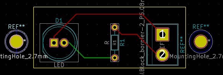
Figure 9.68: The second screw hole is on the right side of the PCB.
The two new footprints are outside the edge cut. View the 3D rendering of the PCB (View, 3D Viewer), and you will see that the new footprints 'exist' outside the PCB.
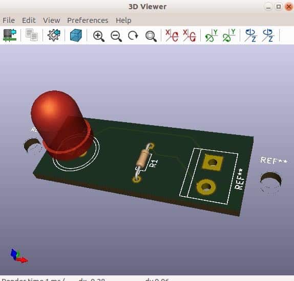
Figure 9.69: The new footprints are outside the PCB; we must redefine the edge cuts.
To fix this, you must redefine the edge cuts drawing. You can do this without deleting the existing edge cut. Let’s work on the left side first. Select the Edge.Cuts layer, and the click on the line graphic button. Zoom in to a comfortable level so that you can make the yellow edge line thick enough. In my example, I work at a zoom level of 13.75. Start drawing a new line from the bottom left corner of the existing edge polygon, as in Figure 9.70.
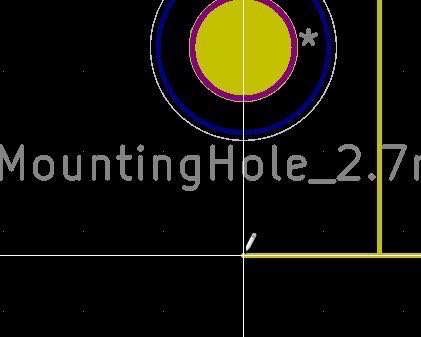
Figure 9.70: Extend the edge cut polygon from a sensible place, like the bottom left corner of the existing edge cut.
Continue the drawing of the new segment of the edge cut until it meets the top left corner of the existing polygon. In the example of Figure 9.71, I have also deleted the vertical segment of the original edge cut polygon. It is good practice to do so in order to reduce the risk of a manufacturer becoming confused. An edge cut polygon should enclose a single area within its sides.
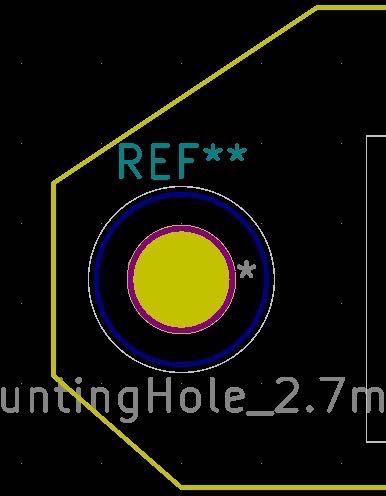
Figure 9.71: The left side of the PCB, redrawn with a new edge cut.
Repeat the same process on the right side of the PCB. Always take care to create polygon line without interrupts, as the polygon must be contiguous. Zoom in and pan as you do the drawing in order to work with larger 'click targets'. Figure 9.72 shows the PCB with the completed edge cut polygon.
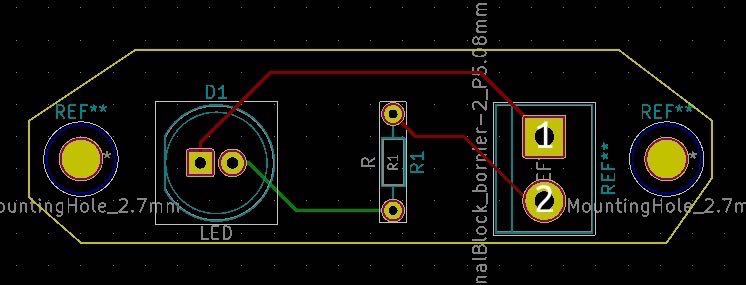
Figure 9.72: The project PCB with its new edge cut polygon.
Use the 3D viewer to see a rendered version of the PCB. In Figure 9.73 you can my PCB, complete with its screw mounting holes and the edge cut extension.
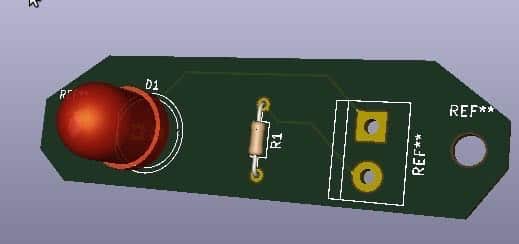
Figure 9.73: The project PCB with its new edge cut polygon, in 3D.
Graphics
With the edge cuts drawing complete, let’s use the same graphics tools to add some cosmetic graphics to the board. Many footprints carry their own graphics in the silkscreen layer. In our PCB, you can see that the LED, resistor and screw terminal already have graphics. You can see them depicted in white, in Figure 9.73.
Let’s add some custom graphical elements.
First, change the layer setting to front silk screen ('F.SilkS'). Then try adding some graphics using the line, circle, and arc tools.
You already know how to use the line tool. I’ve used it to create a box around the LED and the resistor.
To use the circle tool, select it, then click somewhere on the PCB where you would like the centre of the circle to be, and move your mouse to draw it. The further the mouse is from the centre, the larger the circle will be. I have added two circles around the screw holes.
The arc tool is good for drawing parts of a circle. In later projects, we will also use it to create round corners for our PCB, which look better to the eye and are not as sharp. You can use the arc tool similarly to the circle tool, but instead of drawing a full circle it will draw a partial circle. I have added a few decorative arcs on the inner sides of the two screw holes. In Figure 9.74 you can see my PCB art, and in Figure 9.75 its 3D rendering.

Figure 9.74: An example of simple graphics created using the line, circle, and arc tools.
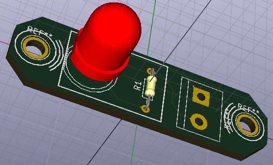
Figure 9.75: A 3D rendering of simple graphics created using the line, circle, and arc tools.
You can also add graphics to the bottom of the PCB. At the moment, there are no graphical elements there. Let’s add a couple of boxes and a circle.
First, select the bottom silkscreen layer ('B.SilkS'). All elements on the PCB will overlap unless you un-select a layer. I find it easier to work with silkscreens when I only have the one I am working on enabled and the other disabled. You can do that from the layers manager toolbar. In Figure 9.76 I have disabled the front silkscreen layer by clicking on its checkbox (in the red box). This hides the silkscreen drawings in the front silkscreen so I can work on the bottom silkscreen layer.

Figure 9.76: When you work in the bottom silk layer you may disable the front silk layer in order to reduce clutter.
In Figure 9.77 you can see my PCB’s silkscreen drawings in purple. I have unchecked the top silkscreen layer to make it easier to see the bottom silk screen elements.

Figure 9.77: The purple line belong to the bottom silkscreen, with top silkscreen disabled.
In Figure 9.78 you can see the 3D rendering of the bottom of the PCB, which shows the bottom silkscreen.
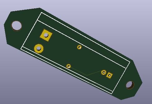
Figure 9.78: 3D rendering of the PCB showing the bottom silkscreen.
In Figure 9.79 you can see the current state of the PCB with all layers visible.

Figure 9.79: The PCB showing top and bottom silkscreen contents.
It is also to add actual graphics to the silkscreen layer of the PCB, not just simple lines and circles. You can have logos, for example, or elaborate artwork. To do so you need to follow a process that involves converting a bitmap graphics file into a footprint, before inserting it into the PCB. You will learn how to do this in the breadboard power supply project.
This PCB is almost complete. There is only one more thing we need to do, and that is to add text to the front and bottom silkscreen.
Text
To add text to the PCB, we can use the Text tool, which is one of the graphics tools marked as '8' in Figure 9.40 . Let’s go right ahead and use it to add your name to the board. Select the front silkscreen layer, and then click on the 'T' button. Click on the location on the PCB where you would like the text to appear. The Text Properties window will appear. Type your name in the Text field, and double check that:
• 'F.SilkS' appears in the Layer drop-down menu,
• 'Normal' appears in the Display drop-down menu.
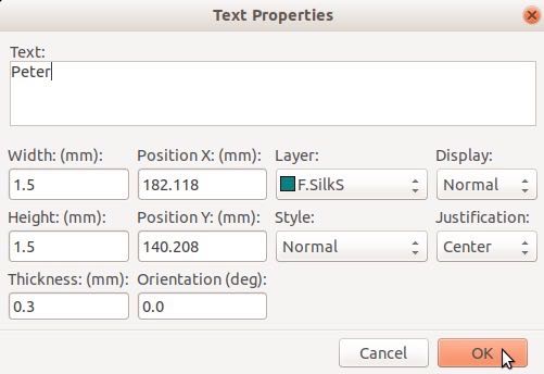
Figure 9.80: The Text Properties window.
You can control the size of the text and its style, but other than that, the text controls are limited. You have the option of placing the text in other layers, including in the top or bottom copper layer. Copper layers are meant to be used for pads and tracks, so unless you have a good reason for this, use the silk layers for text.
If you choose to add text to the bottom layer, take care to set the Display drop-down menu to 'Mirrored'. This will inverse the text so that when it is printed by the manufacturer it is readable.
I will also add text that provides information about the size of the resistor, and also the polarity of the screw terminal pads. This information is very used for the end user of the board. In Figure 9.81 you can see the final top layer silk screen, and in Figure 9.82 is its 3D rendering.

Figure 9.81: Top silk screen with additional text.
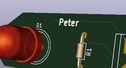
Figure 9.82: Top silk screen with additional text.
The text '330' has a character width of 1 mm. The rest of the characters are 1.5 mm wide each. I placed the '+' and '-' symbols outside the perimeter of the screw terminal so that they remain visible after the screw terminal is soldered on. For the LED, the only use of these symbols is during the assembly, to help me place the LED in the correct orientation. Once the LED is on, the two symbols will be hidden, but that is not a problem since I will not need them anymore.
I will add some text to the bottom of the board, where there is much more space than the front. I typically include a board name, a version number, a date, and my name. Go ahead to add your text, but remember to choose 'Mirrored' in the Display drop-down menu.
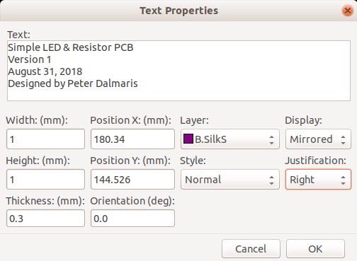
Figure 9.83: The Text Properties, set to print in the bottom silkscreen layer.
I have changed the character width to 1 mm to allow the full text to fit in the available space. I also changed the Layer to B.Silk, the Display to Mirrored, and the Justification to Right. You can use the 'M' hotkey to precisely place the block of text on the PCB, just like you do with any footprint.
Figures 9.84 and 9.85 show the final result.

Figure 9.84: The PCB, with all layers showing enabled.
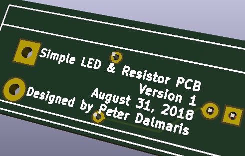
Figure 9.85: 3D rendering of the back of the PCB, with the text clearly visible.
There’s one thing you will need to attend to before we can declare this project complete. With reference to Figure 9.84, notice the text 'REF**' appearing over the screw hole footprints? This isn't text that we would like to include in our manufactured PCBs. Text or other graphical elements that you do not want appearing in the final PCB can be made invisible by editing the item’s properties.
Let’s make the three instances of 'REF**' invisible. Place your mouse cursor exactly over the 'REF**' text of the right screw hole. Then, use the 'E' hotkey to show the text item’s properties window.
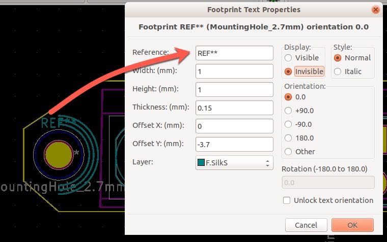
Figure 9.86: To make a text item invisible, edit it’s Display property.
The Display property of the item is right above the OK button. Click on the 'Invisible' radio button, and the 'Ok'.
In Figure 9.88 and Figure 9.87 you can confirm that the 'REF**' instances are now invisible.
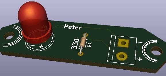
Figure 9.87: The invisible 'REF**' instances are not showing in the 3D rendering.
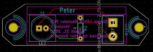
Figure 9.88: The 'REF**' instances are now invisible.
Well done! At this point, your PCB is complete. Make sure you save your work (KiCad does not do this automatically).
You might be wondering, why not go ahead to manufacture this board? While the board you just created is an excellent first project, I’d like you to extend your skills by designing a more challenging board. That board, a simple breadboard power supply, will also be very useful for many of your future projects, so it is an excellent candidate for sending to manufacture.
Let’s complete this section by taking a closer look at the Layer Manager, Status bar and the menus, and then we’ll continue with another project.
Layers manager
You are already familiar with the Layers manager from your work on the simple LED and resistor PCB. The layer manager, apart from allowing you to select the layer on which you would like to work next, also allows you to select which aspects of the layout are rendered.
The Layer manager appears in two different forms. It’s available as a simple drop-down as part of the top toolbar, and in its full-featured variation on the right side of the right toolbar. Because the full layer manager takes up a substantial real estate in Pcbnew, which you may need to use in the layout sheet, Pcbnew provides a button in the right toolbar that allows you to show or hide the layers manager toolbar.
You can see all this in the example of Figure 9.89.
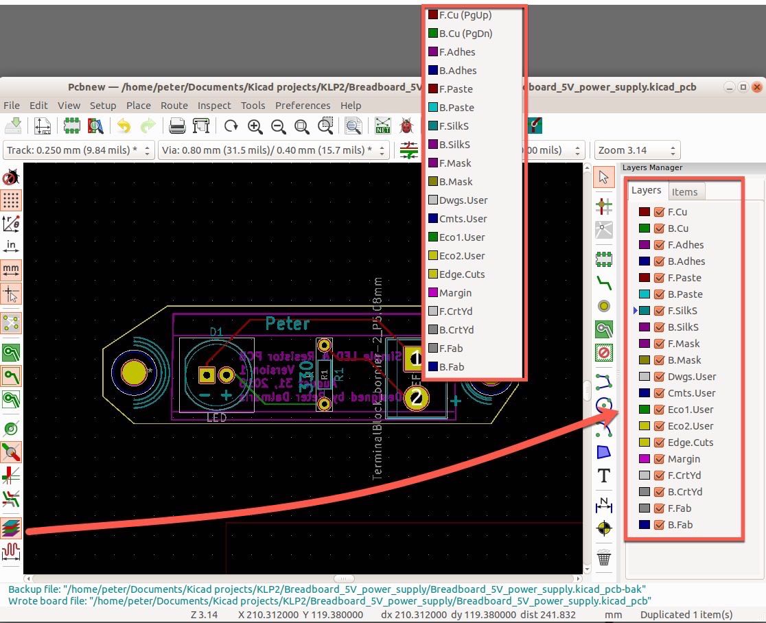
Figure 9.89: The two variation of the layer manager, and the show/hide button.
The drop-down version of the layout manager and the Layer tab of the toolbar version are almost identical. They both allow you to select the current layer. But the toolbar version also allows you to hide or show the items that belong to a layer. For example, to make the tracks drawn in the front copper layer, just un-check the F.Cu option. The red track in our small PCB will disappear.
Try hiding the items in the front and back silkscreen layers as another example.
Hiding and showing layer items is not possible through the drop-down version.
The toolbar version also has a second tab, titled Items (Figure 9.90).
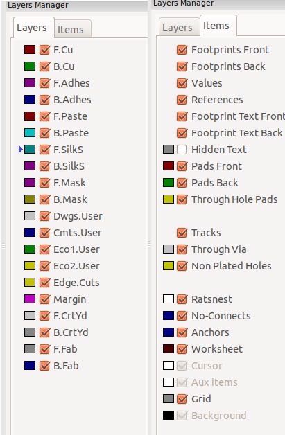
Figure 9.90: The Layer (left) and Items (right) layers of the Layers Manager toolbar.
In the Items tab, you can control the visibility of additional items of your PCB. For example, try un-checking the 'Text Front' item. This will make text to disappear, even if it belongs to multiple layers. Experiment with some of the other options in the Items tab, including the Grid option. When you check and uncheck the Grid option, notice how the Grid button (at the top of the right toolbar) updates its state.
Status bar
The status bar appears in the bottom of the Pcbnew window. It contains two segments. The top one displays the properties of the currently selected item, which the second one shows coordinates, distance, and zoom information.
Let’s have a look at an example. In your simple LED and resistor PCB, click on the LED footprint. The properties of the LED footprint will appear in the status bar (see Figure 9.91).

Figure 9.91: The selected LED footprint with its properties displayed in the status bar; the coordinates of the mouse pointer are also displayed in the status bar.
This way, you can quickly get information about footprints, tracks, text and graphical items.
A very useful feature of the status bar is distance counter. You have seen this feature before, in Eeschema. It works in the exact same way in Pcbnew. Let’s look at an example.
What is the width and height of the PCB you have just designed, in millimeters? We can measure it. Please your mouse pointer on the left extreme of the PCB, press the spacebar to reset the counters, and move it to the right extreme. The dx counter will show a value of 44.50 mm. The dy shows a value of -0.25 mm because I move my pointer down during the measurement (Figure 9.92).
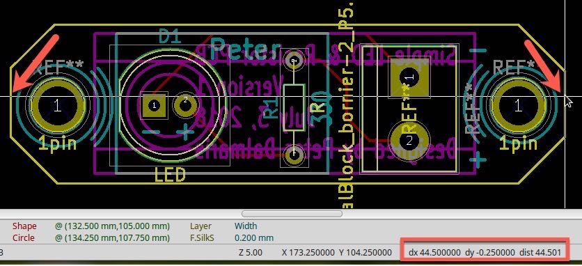
Figure 9.92: The width of this PCB is 44.50 mm.
Do the same on the Y axis to find out the height of your PCB. The height of my PCB is 12.75 mm (Figure 9.93).
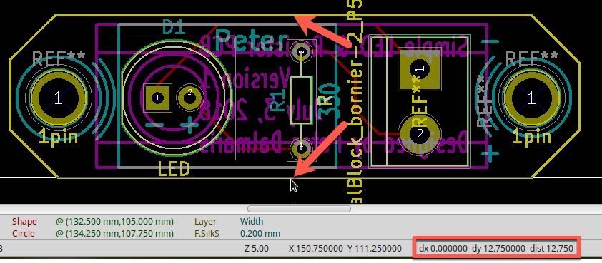
Figure 9.93: The width of this PCB is 44.50 mm.
Just like the status bar in Eeschema, the status bar in Pcbnew also provides information about absolute cursor coordinates, the zoom level, and the distance unit selected.
Menus
To complete our tour of Pcbnew, let’s have a quick look at the menus.
The first thing to notice is that many of the functions that are available through the toolbars are also available through the menu system. For example, in the File menu, you will find options for printing, editing the page settings, plotting and saving the layout, and in the View menu, you will find options to zoom in/out, redraw and fit the layout to screen.
All of the menus except for Place, contain unique functionality. In this segment, we’ll review the most commonly used of those functions.
File
In Figure 9.94 you can see the contents of the File menu.
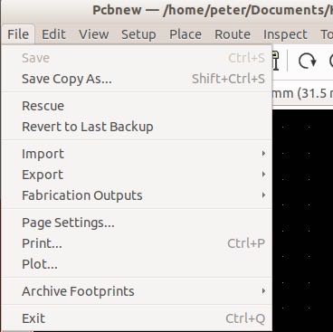
Figure 9.94: The Pcbnew Edit menu.
You should be able to recognise many of the items in it:
- Page Settings, allows you to edit the contents of the title block and the page layout, as you have already learned.
- Print, allows you to print the layout on paper.
- Export, allows you to export the layout in various formats. For example, you can use the SVG files (one per layer) in third-party drawing applications, and Specctra DSN for using external autoroutes that support this format (such as FreeRouting, which you can learn about in a relevant recipe).
- Plot, allows you to export the layout to a format appropriate for sending to a manufacturer, like Gerber. Interestingly, you can also use Plot to export to SVG, PDF and other formats. All of those can be used to manufacture the final PCB.
- Close, to close Pcbnew.
Apart from the above, several functions available through the File menu are new:
- Save a Copy As…, allows you to save the layout under a new file name. This is useful when you want to branch out your layout. For example, you can have one layout designed to use surface mounted components with the file name 'LED_resistor_smd.KiCad_pcb', and another with the file name 'LED_resistor_th.KiCad_pcb'.
- Revert to Last Backup, allows you to load the layout recovery file. Pcbnew automatically saves your work every 10 minutes. This value is configurable via the Preferences, General window. The backup file has the '.KiCad_pcb-bak' extension. When you click on Revert to Last, Pcbnew will ask you to confirm that you want to revert to the content of the backup file and replace your current work.
- Rescue, allows you to load an automatically created backup. By default, Pcbnew will back up your work every 10 minutes. You can control the interval through the General Settings window, from the Preferences menu item. I personally save my work manually every couple of minutes, and commit to the project Git repository and prefer not to rely on KiCad’s autosave function.
- Fabrication Outputs, give you access to several types of file formats that can be used in a PCB fabrication process. In this book, you will learn how to export for manufacturing using the industry-standard Gerber files.
- Import, allows you to import Specctra auto routing and DXF (Drawing Exchange Format) files that contain CAD models. DXF is a format developed by Autodesk. With it, for example, you can create a layout of a PCB placement in a program like Fusion 360 and import it into KiCad.
- Export, allows you to export layout data to Specctra, GenCAD (a file format used in PCB manufacturing and testing), IDFv3 (a PCB file format) and others. These file formats make it possible to use KiCad PCB projects with other CAD software. Unless you have a need to inter-operate with third-party CAD software, you are unlikely to need to venture into this menu.
- Archive Footprints gives the ability to package the footprints found in a layout in a directory within your project so that you can share the project with your collaborators. Your collaborators will be able to work with your project even if they don’t happen to have the needed footprint libraries installed.
Let’s have a look at the functionality found in the Edit menu next.
Edit
In Figure 9.95 you can see the contents of the Edit menu.
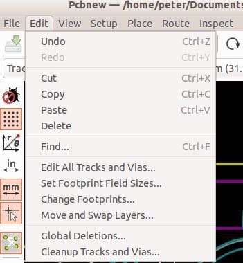
Figure 9.95: The Pcbnew Edit menu.
In the Edit menu you can see the standard Undo, Redo, Delete and Find buttons, but in addition, there are several more buttons that are worth a closer look.
In summary:
- Global Deletions, which allows you to delete all items of a specific kind.
- Cleanup Tracks and Vias, which allows you to clean up stray items, like unconnected tracks and redundant vias.
- Move and Swap Layers, which allows you to swap a layer with any other layer.
- Set Footprint Field Sizes, which allow you to set default properties for footprint text values.
The Global Deletions window provides a quick and efficient way to remove all items of a specific kind of items from the layout. This is one of those features that you will use rarely, but that will save you a lot of time when you need them. While it is a blanket approach to removing items, remember that you still have access to the Undo function, so if you make a mistake you can restore your work.
Try to be selective, when you use Global Deletions. Selecting the 'Clear board' radio button will delete everything in the layout. Selecting 'Text' will only delete the text items. You can also apply your choice to a specific layer or to all layers.
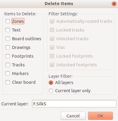
Figure 9.96: The Global Deletions window.
The Cleanup Tracks and Vias windows help us tidy up leftover tracks and vias, quickly. Try this experiment. In your LED and resistor layout, add a few stray tracks. As you are laying a track, type 'V' to add a via, and continue drawing. Double-click to end drawing. Don’t connect the stray track to any pads. That is what makes it 'stray'. Now, bring up the Cleaning Options window by clicking on Edit and Cleanup Tracks and Vias. Leave the current default selections as they are, and click OK.
The stray track and vias that you just added should disappear.
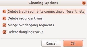
Figure 9.97: The Cleaning Options window.
The Swap Layers function (Figure 9.98) is very useful when you want to transfer all tracks from one layer to another. For example, say that you want to move all track from the front copper layer ('F.Cu') to the bottom copper layer ('B.Cu').
To do that, first bring up the Swap Layers window by clicking Edit and the Swap Layers. Then, click on the button marked '…', right next to the 'F.Cu' label, and from the small window that appears, select 'B.Cu', then dismiss the small window by clicking on the 'x' button, and click OK. Try that now in your LED and resistor layout. See how the (originally' red tracks are now green? That happened because the tracks were transferred from the front copper layer to the back copper layer.
To restore the tracks to the front copper layer, do the opposite. Back in the Swap Layers window, click on the '…' button that is next to the 'B.Cu' label, and select 'F.Cu' from the small window that appears. Then, dismiss the small window and click OK.
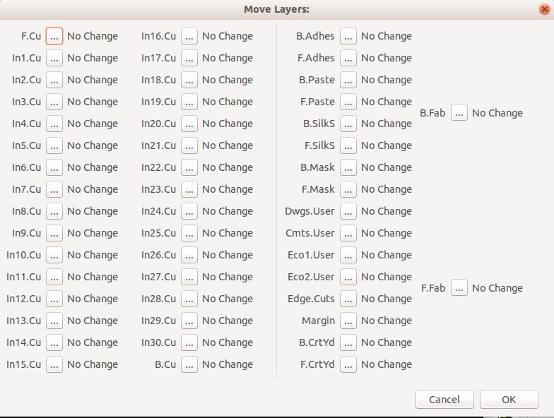
Figure 9.98: The Swap Layers window.
In Figure 9.99 you can see the Set Text Fields window. The width, height and thickness properties control how the footprint text values are rendered in the editor. Do a small experiment to see how this works: With the simple LED and resistor layout loaded in Pcbnew, bring up the Set Text Size window. Change Width and Height to 2, and Thickness to 0.35. Click OK. You should see that all text items that belong to properties will be re-drawn with the new properties, and look around twice as large. To make them go back to their original sizes, restore Width and Height to 1, and Thickness to 0.15.
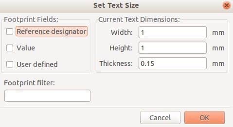
Figure 9.99: The Set Text Size window.
View
In Figure 9.100 you can see the contents of the View menu.
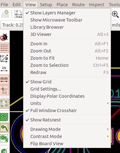
Figure 9.100: The Pcbnew View menu.
In the View menu you can see the familiar Zoom, Fit and Redraw buttons, but in addition, there are several more buttons that I’d like you to look at.
- 3D Viewer, which renders a 3D view of the PCB
- Show Ratsnest, which shows you a list of all unconnected nets in the PCB
- Drawing Mode, which allows you to choose from a variety of graphics options that help when you work on busy boards
You have already used the 3D viewer in several occasions (Figure 9.101). Apart from the default settings of the viewer, there are several more features you should be aware of. First, experiment with the top menu bar, which allows you to zoom in/out, pan and rotate the model.
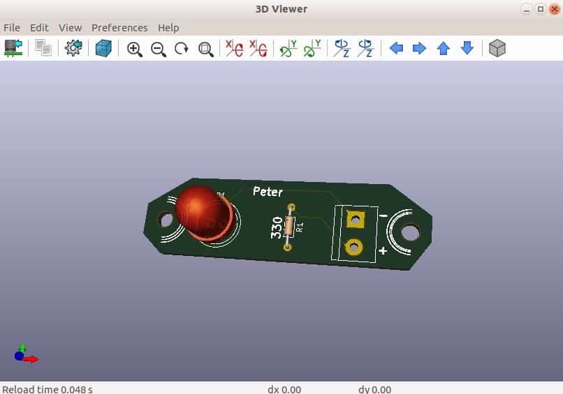
Figure 9.101: The 3D Viewer.
You can control much of the rendering behavior of the viewer through its display options window, which you can access by clicking on the cog-wheel button in the top toolbar (Figure 9.102). Try out the various options to see the effect they have on the rendering of the model. There are more rendering controls through the Preferences menu.
Another useful function is available in the File menu. There, you can export the rendered view to PNG or JPEG image files. This is a good way to capture a high-quality render of your board that you can insert in a blog post or documentation.
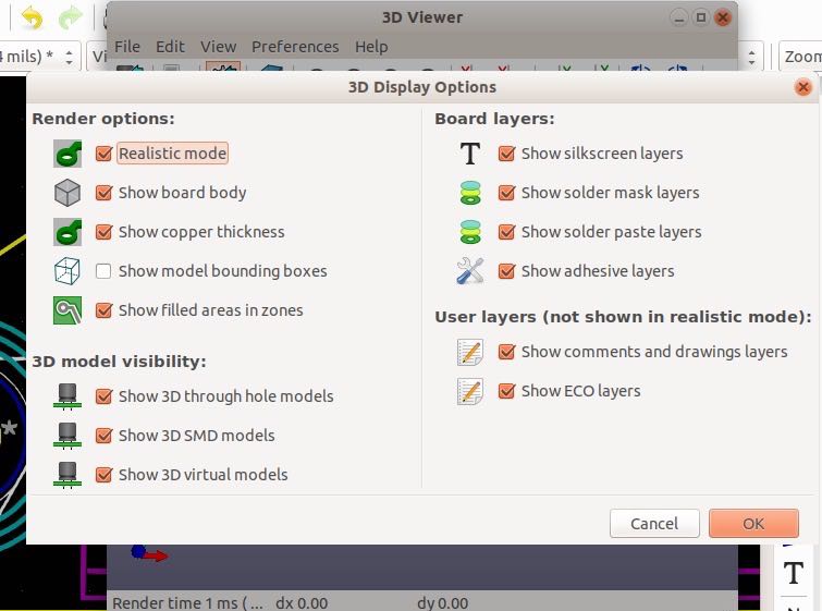
Figure 9.102: The 3D Viewer’s display options window.
Setup
The Setup menu contains just two items, Design Rules and Layers Setup. You can see the Setup menu in Figure 9.103.
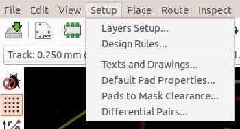
Figure 9.103: The Setup menu
The two most important items in this menu are the top two: Layers Setup and Design Rules. You will use them in all projects of this book. You can read a summary of what these items do in the next few pages.
The bottom four items allow you to configure secondary aspects of how the layout, such as how text should look like by default, and what should be the default configuration of a pad.
Let’s take a closer look at those.
Design Rules Editor
In the Breadboard Power Supply and later projects, you will be spending a lot of time learnings on how to use the Design Rules Editor. Briefly, this Editor allows you to create classes of nets that have specific design attributes. Tracks that belong to those nets are then drawn with adherence to this attributes.
For example, you can create a net class called 'PWR' that dictate the track width, via diameters and other attributes that should apply specifically to a track that belongs to this class. You could create another class called 'SGN' that dictate these attributes for tracks that convey signals, instead of power. This makes sense because a typical signal track will only need to convey a few milliamps of current, while a track that feeds power to the circuit components will be required to convey much more than that.
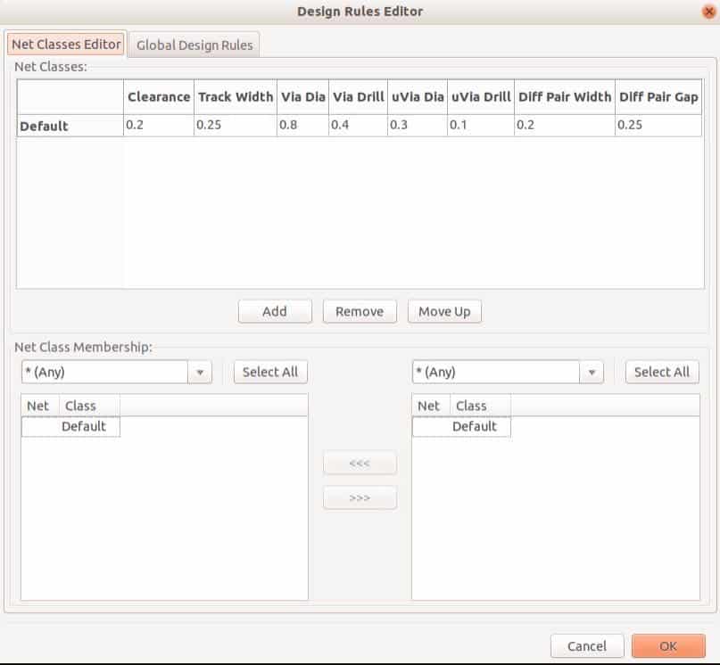
Figure 9.104:The Net Classes Editor.
In Figure 9.104, you can see Net Classes Editor with its default values. In our simple PCB, there’s only one net, and it is assigned to the Default class. In later projects, you will learn how to create classes and assign nets to one of them.
In the same figure, there is also the Global Design Rules tab (Figure 9.105) .
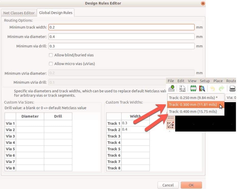
Figure 9.105: The Global Design Rules.
There, you can create custom track and via sizes, and have them available in the top toolbar drop-down. This way you can create tracks and vias using ad-hock sizes that can override their assigned class.
Layers Setup
In Layers Setup (Figure 9.106), you can control the number of layers you would like your board to have, and, to some extent, the type of these layers.
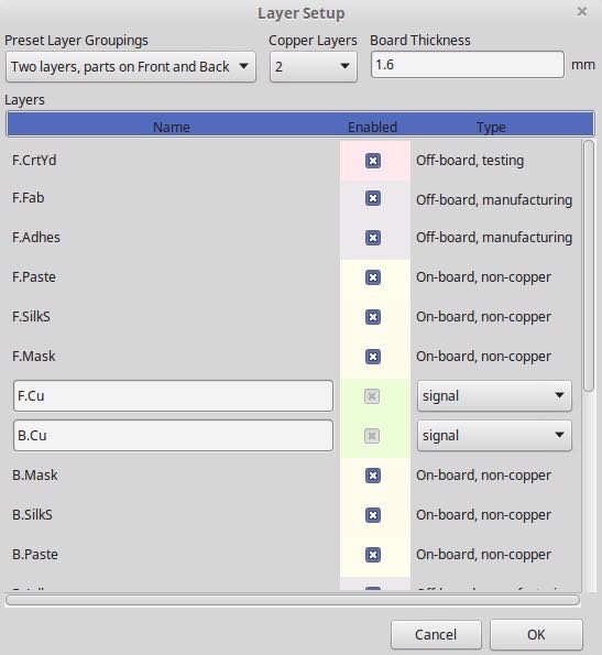
Figure 9.106:The Layers Setup.
Pcbnew can produce PCBs with up to 32 copper layers, and this is configurable in the Layers Setup window.
There are presets of up to four layer-PCBs with parts on the front, back, or both. As you experiment with selecting one of them, notice the effect on the enabled or disabled status of each layer. For example, if you choose the 'Two layers, parts on Front only' preset, you will notice that many of the copper layers are disabled. If you click on 'OK' to commit the change, these layers will disappear from the Layers Manager, leaving only the enabled ones showing.
You can change the layer configuration as you are working on your PCB. For example, you may start with a 2-layer PCB and then realise that you need additional layers to complete the routing. That is not a problem. Just go into the Layer Setup window and add a couple of layers.
Other setup options
The bottom four options of the Setup menu contain:
- Text and Drawings
- Default Pad Properties
- Pads to Mask Clearance
- Differential Pairs
The Text and Drawings settings allow you to configure defaults for things like the text character width, height and thickness, and the thickness of a graphic segment (such as a line or an arc).
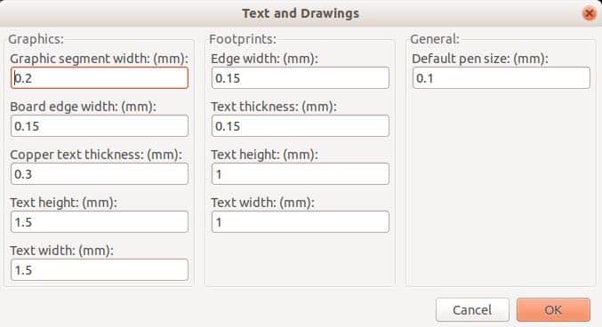
Figure 9.107: Default text and graphics settings.
I find the defaults in Figure 9.107 appropriate for most boards.
The Default Pad Properties is fairly involved, but you only need a few options tweaked in relation to setting defaults (Figure 9.108).
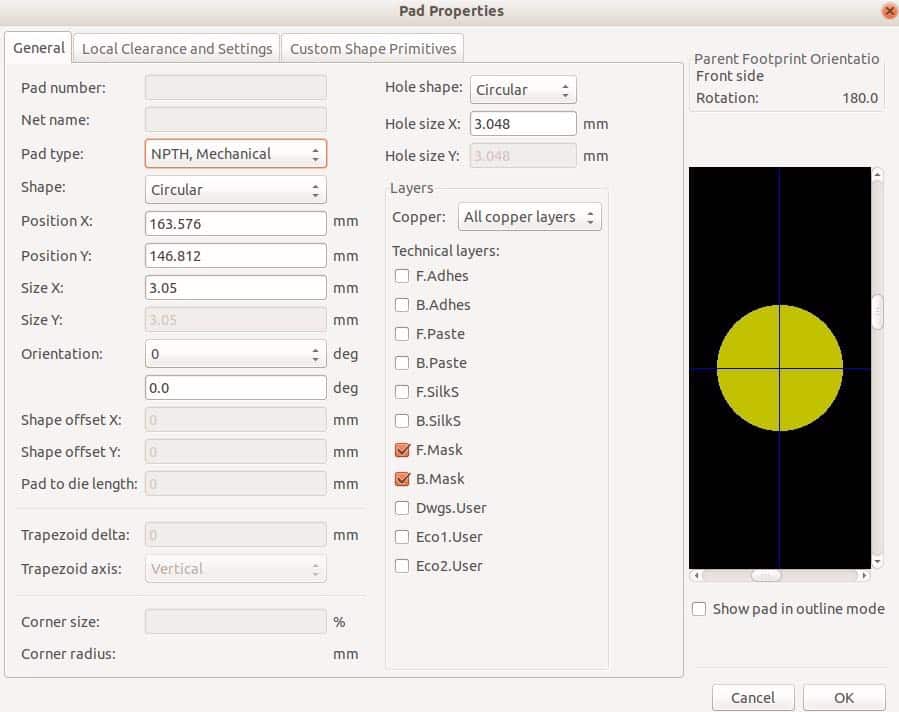
Figure 9.108: Default pad properties.
In the General tab, the pad type offers four choices:
- Through-hole, best for using with through-hole components. This option creates a hole that is internally plated, with pads on either side so that components can be soldered.
- SMD, suitable for SMD components. An SMD pad does not contain a hole.
- Connector, which is similar to the SMD type, but is round and typically used as a contact for probes
- NPTH, Mechanical, which is a non-plated through hole pad, suitable for creating mounting holes.
If you choose 'Through-hole' as your default, you will also be able to specify the hole shape, as either oval or circular, and for each type, the exact dimensions.
In the Local Clearance and Settings tab you can specify minimum clearances (Figure 9.109). I prefer to keep the values there at 0 so that the footprints in my projects inherit these values from their parent footprints.
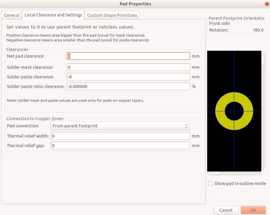
Figure 9.109: The Local Clearance and Settings pad
The Pads Mask Clearance window (Figure 9.110) allows you to control the pad mask clearance. The mask is the thin layer of non-conductive materials that covers the front and back of the board and also prevents solder from creating bridges between pads. The values you use here control how much of the pad will be covered with the masking material. If you cover too much, you will decrease the risk of solder bridges, but you will make soldering harder since there will be less of the pad exposed.
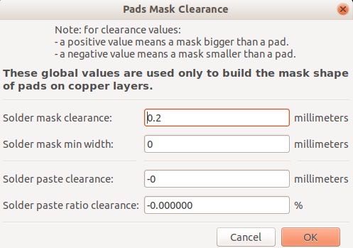
Figure 9.110: The Pads Mask Clearance window.
Finally, the Differential Pair Dimensions allow you to control how close together will be drawn traces that belong to the same pair, and how wide each trace should be.
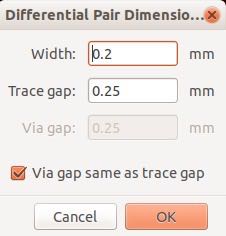
Figure 9.111:Differential pair settings.
Place
In Figure 9.112 you can see the contents of the Place menu.
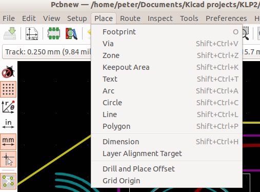
Figure 9.112: The Pcbnew Place menu.
In the Place menu, you will find the same tools as in the right toolbar. Let’s not spend any more time here and move straight to the Route menu.
Route
In Figure 9.113 you can see the contents of the Route menu.
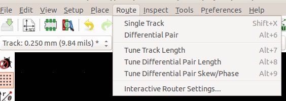
Figure 9.113: The Pcbnew Place menu.
With the Single Track option, you can create regular tracks and vias. It is the option you will use most often. The rest of the tools in the Route menu are useful in advanced layouts that involve things such as high-frequency digital busses or analog circuits where the radio properties of the tracks must be taken into account.
Let’s have a quick look at each one:
- Single Track, allows you to create single tracks and vias. You have already used this tool in our simple LED and resistor project.
- Differential Pair, allows you to route two tracks at the same time. KiCad identifies tracks that should be routed together based on the ending of their net names. In the current version 5, two tracks can be identified as a pair if their net names end with '+' and '-' respectively, and their start pads are adjacent to each other. While you are drawing the paired tracks, you can also create vias, for both at the same time.
- Tune Track Length, allows you to adjust the exact length of a single track. This is useful if you want to control precisely the signal propagation time.
- Tune Differential Pair Length, which is a function similar to Tune Track Length, but for a pair of tracks ('differential pair') at the same time.
- Tune Differential Pair Skew/Phase, allows you to precisely control the clock skew of differential pairs, another consideration in high-frequency digital electronics design. Clock skew is a phenomenon in which the same clock signal arrives at slightly different times to its destination. The effect of this is that different parts of the circuit can end up operating at a slight clock offset, which is not desirable. Learn more about clock skew on Wikipedia.
For example, we can use Differential Pairing for tracks that involve serial communications, such as the TX and RX tracks in a UART circuit, or the MISO and MOSI tracks in an SPI circuit. You can learn more about differential pairs in the recipe titled 'How to use differential pairs'.
Interactive Routing
Interactive routing is one of the most important features of Pcbnew. It makes drawing tracks quick and efficient.
It helps you create tracks while avoiding items in the layout that can’t be moved, or moving them (the term is 'shove') if they are movable.
Let’s do an experiment with Interactive routing. Open the simple LED and resistor layout, and delete the track that connects pad 2 of the LED and pad 1 of the resistor. In Figure 9.114, I have deleted the track. To make the layout easier to read, I have disabled the front and back silkscreen layers by unchecking F.SilkS and B.SilkS in the Layer Manager.

Figure 9.114: The resistor and LED are not connected.
The ratsnest line between the LED and resistor is telling us that this track must be implemented. Type the 'X' hotkey to enter the track drawing mode. Place your mouse cursor in the middle of pad 2 of the LED. Move your mouse towards the screw terminal footprint, and notice how the track that the router leaves behind does not intersect any other tracks and goes around pads. Try to finish the drawing by double-clicking on pad 1 of the resistor. You can see my, admittedly terrible, design in Figure 9.115.

Figure 9.115: A new route using the Interactive Router, avoiding other tracks and pads.
In Figure 9.115, I have highlighted the new net using the 'Highlight Net' button in the right toolbar. Of course, this new net is a very poor design since it is much longer than necessary, with a lot of corners. In PCB design, we aim to create tracks that are as short as possible, with as few corners as possible. More about PCB design principles later.
The point of this example is that as I was moving my mouse pointer through a particular path, the Interactive Router was able to find a way to place the track without violating any of the design rules.
You have fine control over the designer through the context menu Figure 9.116.
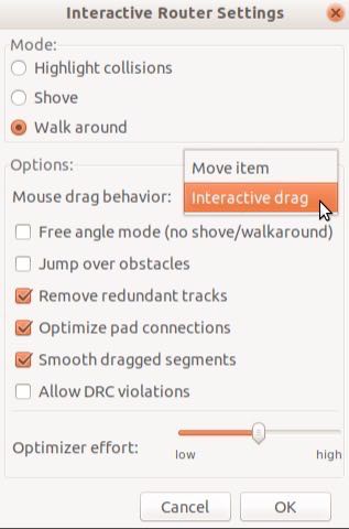
Figure 9.116: The Interactive Router Settings.
You can change these setting at any time, even during the drawing of a track. I usually set the Mode to 'Walk around', which produces a result similar to the one you see in Figure 9.115. As long as you choose a sensible path with your mouse, the interactive router will produce a sensible track. You can also try out the Shove mode. With Shove mode on, the interactive router will push over any items that are not explicitly fixed on the layout. You can have footprints on a fixed position by locking them through their properties and then allow for existing tracks and vias to be moved by the router as needed for laying new tracks. It is work spending some time to get used to this feature, as it is powerful and it will make your work with KiCad much more efficient in comparison to drawing in Default mode without Interactive Routing.
In Figure 9.116 I have selected the option 'interactive drag' for the mouse drag behaviour. This allows me to use the 'G' hotkey to drag a track to a new position without breaking it (which is the 'move' operation). Beware that you can drag a track by clicking on it to select it and then dragging to move it. The ‘G’ hotkey is a shortcut meant to save you one click. This way I can re-arrange a track that I or the Interactive Router created, without having to repair broken connections. When using the 'Move' method, the typical result is that a single segment of a track is moved, and its connection to the rest of the net is broken, which needs to be repaired.
Another powerful feature of the Interactive Router is the ability to redefine a segment of the track or the full track without having to manually delete the original. You simply type 'X' to start the track drawing process, and you draw the start and end of the new track or track segment. When you double-click to finish the drawing process, the Interactive Router will automatically remove the old track or track segment, as it is now redundant.
Let’s use this feature to repair my awful track from Figure 9.115. Type 'X' and click on pad 2 of the LED to start a new track. You can also start the drawing at another position of the existing track is you want to redefine a segment of the track instead of the complete track (Figure 9.117).
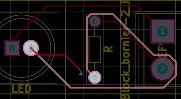
Figure 9.117: Starting a new track to replace the old one.
Then, move your mouse on pad 1 of the resistor and double-click to complete the drawing. The new track is created, and the old track is automatically deleted (Figure 9.118).
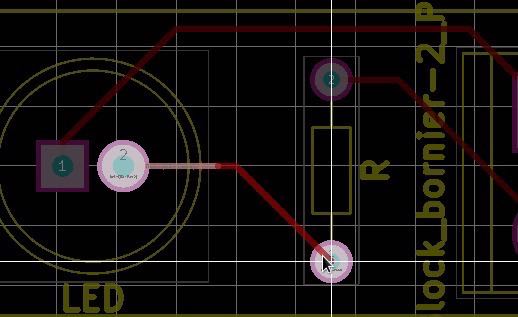
Figure 9.118: The newly created track replaces the original.
It is worth spending some time here to get used to these capabilities of the Interactive Router. We will be using it extensively in the projects that will follow.
Inspect
The Inspect menu (Figure 9.119) includes functions for looking into nets, measuring distances on the sheet, and launching the design rules checker. You can do the latter two by using buttons in the top and right toolbars.

Figure 9.119: The Inspect menu.
The List Nets options give you a list of the nets that are present in the PCB. In Figure 9.120, you can see the Nets window. You can type in the name of the net you want to inspect in the filter box or click on the net row. In Pcbnew, whichever net you select will be highlighted.
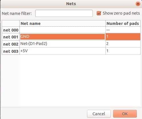
Figure 9.120: The Net Filter window.
In Figure 9.121 you can see the GND net that I selected in Figure 9.120, highlighted with a high-contrast colour. This makes it easy to see how the selected net is routed
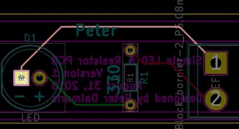
Figure 9.121: A list of nets present in this simple PCB.
With the Measure tool, you can measure distances on your board (Figure 9.122). Notice that there is a keyboard shortcut for this tool. Just click to start measuring distance and angle, and click again to end. You can use this tool by clicking on the Measure tool button from the right toolbar.

Figure 9.122: The Measure tool.
Finally, you can start the design rules check by clicking on the Design Rules Checker option in the Inspect menu, or by clicking on the bug button from the top toolbar. Either way, the DRC window will come up (Figure 9.123).
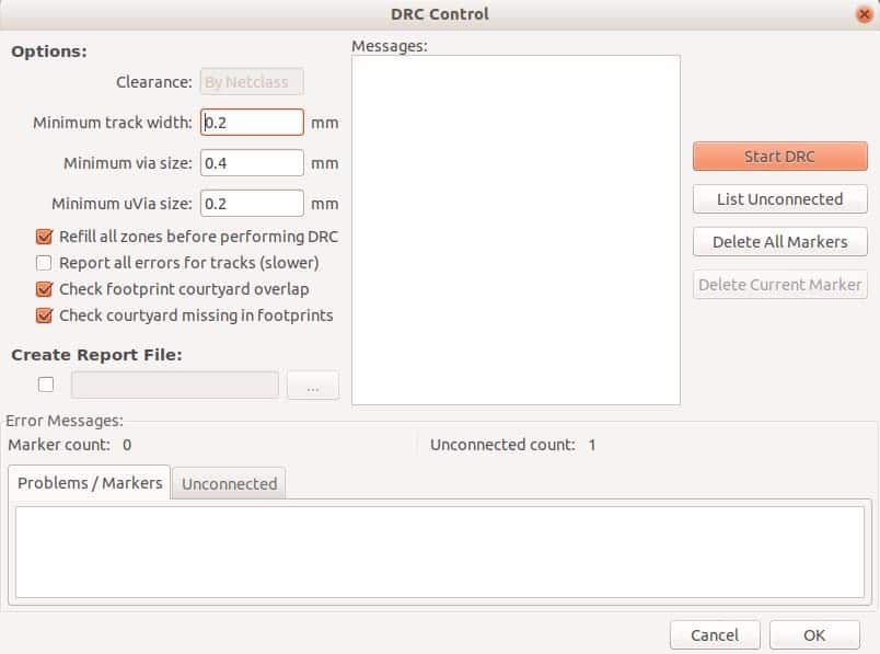
Figure 9.123: The DRC tool.
The DRC tool will check for problems in your PCB, such as unconnected nets, or traces that are too close to other traces. You will become very familiar with this essential tool as you practice working on the projects in this book.
Tools
All but one of the items in the Tools menu are available in the top toolbar. You can see the Tools menu in Figure 9.124.
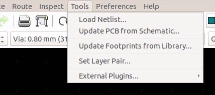
Figure 9.124: The Tools menu.
Here is a summary of the items in the Tools menu.
- Load Netlist, allows you to import the Netlist file from Eeschema.
- Update PCB from Schematic is an alternative to the Netlist. If you make changes to the schematic after you begin work in Pcbnew (perhaps you have added a new symbol, or fixed the wiring), you can choose the Update function to automatically annotate the symbols, create the new netlist, and import it into Pcbnew. I am very used to working with the Netlist directly, so I don’t use the Update function, however, I suggest you give it a go as it can speed up your work.
- Set Layer Pair, is useful in boards with 4 or more lairs. It allows you to choose which layer should be connected when you create a via.
- Update Footprints from Library, will check for updated versions of the footprints that exist in your layout, and apply them. This saves you doing this work manually, as was the case with older versions of KiCad.
- External Plugins allows you to extend the capabilities of KiCad through Python scripts.
I’d like to take a closer look at the Set Layer Pair option.
Let’s start with the Layer Pairs option. When you work with PCBs that contain more than 2 layers, say 4, or more, you can configure which of these layers should be considered pairs when you create vias. You can configure the Layer Pairs using the Select Copper Layer Pair window. When you are working on a 2-layer board, the Select Copper Layer Pair window looks like the example in Figure 9.125. There’s not much to do here, and the only option is to pair the top and bottom layers. Now, when you create a via, a track from the top layer will continue to the bottom layer, and vice versa. The 'x' marks the selected layer.
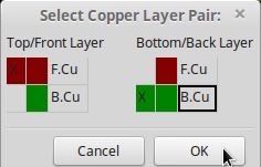
Figure 9.125: The Select Copper Layer Pair window in a two-layer board.
Change your board configuration so that it is a four-layer board. You can do that through the Design Rules menu (we will look at this in more detail in the next segment). Bring up the Layers Setup window, and change the number of layers to 4 (Figure 9.126).
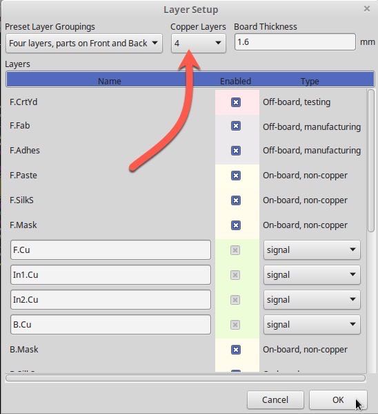
Figure 9.126: To change your board to a four-layer board, open the Layer Setup window from the Design Rules menu.
Now open the Select Copper Layer Pair window again. It will look like the example in Figure 9.127.
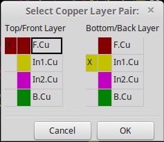
Figure 9.127: The Select Copper Layer Pair window in a four-layer board.
In this example, I have set the pairs to be the front copper and the first inner copper layers. With this configuration, when I create a via, a track that starts in the top copper layer will continue in the first inner copper layer, and vice-versa.
Please switch your board back to a two-layer configuration now before continuing.
Preferences
Through the Preferences menu, you can control various aspect of the operation of Pcbnew (Figure 9.128).
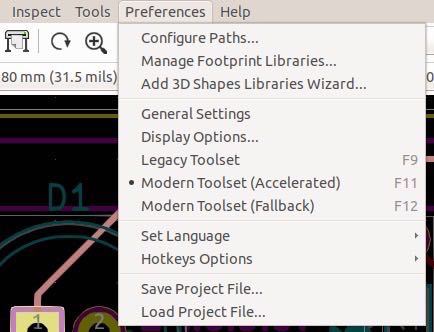
Figure 9.128: The Preferences menu.
You will be using most of the items in the Preferences menu as you work through the projects in this book, but following is a summary:
- Manage Footprint Libraries Wizard, allows you to import footprint libraries. Once a new library is imported, you can use its footprints in your layout. You will learn how to use this tool in a later project in this book. There is also a recipe that explains how to do this; look for the one titled 'Adding a footprint library in Pcbnew'.
- Configure Paths, allows you to configure the locations of symbol, footprint, and 3D shape libraries. You can also access the path configuration window from the main KiCad window. Look at the Kicad documentation for details on the roles of the environment variables and the paths that they point to.[7]
- Add 3D Shapes Libraries Wizard, allows you to download 3D shapes from KiCad’s own repository and 3rd party repositories that are used in Pcbnew’s 3D Preview. You can learn how to do this by reading the recipe titled 'How to install 3D shapes'.
- General settings, allow you to control a variety of aspect of Pcbnew’s operation, such as the frequency of the autosave function, the measurement units and type of coordinate system used.
- Display options, allow you to control Pcbnew operations details such as the use of accelerated graphics, the grid style and how net names are displayed.
- Set Language, allows you to change the language used in the Pcbnew user interface.
- Hotkeys Options, allows you to customise the various hotkeys, as you learned earlier.
- Save and Load project File allows you to save the .pro file that contains information about the project (but not the layout and schematic files, since that information is stored as individual files).
- There are recipes that cover the usage of the libraries wizard and the 3D shapes wizard. In the next few pages, you'll take a closer look at some of the other options in the Preferences menu.
General
Through the General Setting window (Figure 9.129), you can configure much of the behaviour of Pcbnew.
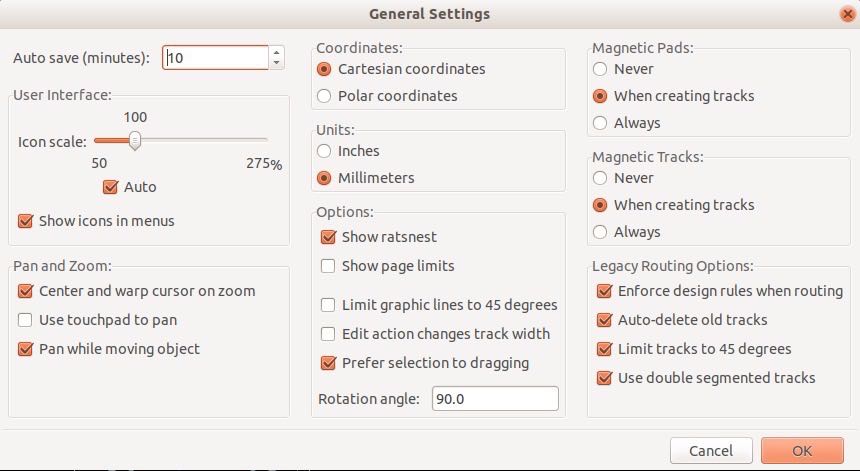
Figure 9.129: The General Setting window
Here, you can control the drawing behavior of Pcbnew. For example, you can make tracks and pads 'magnetic' so that as you draw a new track, it will 'stick' to a pad when you mouse your mouse close enough, ensuring an electrical connection.
You can control autosave, select your preferred coordinate system and unit of measurement, the shape of the course, and much more.
I find that the default settings work well and rarely make any customisations here.
Display
Similarly to the General Settings window, the Display Options window (Figure 9.130) allows you to control the graphical attributes of Pcbnew.
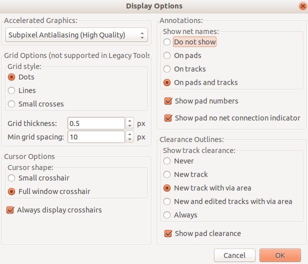
Figure 9.130: The Display Options window.
For example, you can choose if you would like to show pad numbers and footprint outlines, net names, and track clearances.
Again, the default settings are reasonable and I prefer not to make any modification to the Display options.
Language
The Language option allows you to choose one of 19 languages available for KiCad’s user interface. Whichever language you choose, must also be supported by the locale of your operating system (Figure 9.131).
Figure 9.131: The Pcbnew language settings have to match the locale of your operating system.
Hotkeys
You have learned about the Hotkeys options in earlier segments of this book. You know that you can show the current hotkeys by selecting Preferences, Hotkeys, and List Current Keys and that you can set up your own hotkeys through Preferences, Hotkeys and Edit Hotkeys.
You can also import and export hotkeys from the same menu item, which is a good way to ensure that you have the same settings across the computers where you use KiCad.
Notes
[4] The Crazyflie is an open-source flying robotics platform. Visit the project website to learn about the amazing products and projects that are based on Crazyflie: https://www.bitcraze.io/crazyflie-2/
[5] I remind you that a 'net' describes an electrical connection in Eeschema and in Pcbnew. A track is the implementation of this connection. The track retains the name of the net.
[6] A raw PCB is covered with a layer of copper. Using an etching chemical process, the copper is removed so that only the needed traces are left behind.
[7] http://docs.kicad.org/master/en/kicad.html
KiCad series
Ready to learn KiCad?

Learn the world's favourite open-source PCB design tool with the world's most comprehensive course
KiCad Like a Pro, 3rd edition is available as a video course or as an eBook.
Choose the version that fits best with your style of learning, or get both to get the full benefit of the video demos plus the details of the eBook.
When you complete KiCad Like a Pro 3e, you'll be able to use KiCad to design and manufacture multi-layer PCBs with highly integrated components and a professional-looking finish.
Work through five projects that give many opportunities to learn and practice all of KiCad's important features.
KiCad Like a Pro 3e contains full sections dedicated to PCB and design principles and concepts. These ensure that you will master the fundamentals so that your PCB project are awesome.
If you are someone who is interested in designing PCBs using KiCad, or moving to KiCad from another CAD application, then KiCad Like a Pro, the video course and eBook, is for you.
Jump to another article in this series.
Last Updated 4 years ago.
We publish fresh content each week. Read how-to's on Arduino, ESP32, KiCad, Node-RED, drones and more. Listen to interviews. Learn about new tech with our comprehensive reviews. Get discount offers for our courses and books. Interact with our community. One email per week, no spam; unsubscribe at any time
