8. A hands-on tour of KiCad with a very simple project
Schematic design in Eeschema
Schematic design in Eeschema
You are now in Eeschema and looking at an empty sheet, as in Figure 8.1. The annotations help us walk through Eeschema’s menus items.
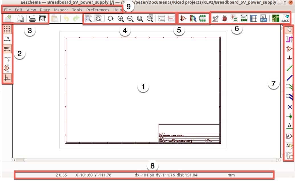
Figure 8.1: An empty Eeschema sheet.
Let’s become familiar with Eeschema by taking a quick tour around its various buttons, menus, and controls. Eeschema consists of the sheet area in which you compose your schematic (1), multiple menu bars (2, 3, 4, 5, 6, 7), the status bar (8), and the menus (9).
Let’s have a look at the useful mouse and keyboard controls before we look around the Eeschema user interface.
The schematic sheet
In Eeschema, you create schematics inside the sheet area. As is typical with engineering documents, at the bottom right corner of the sheet is the title block. The title block contains information about your schematic, such as its name, the name of its author (you!), and the date of the last edit.
In Figure 8.2, I have edited the title block to contain some example information. You can add as much or as little information as you wish. At the very least, I provide a title, the author name, revision, and a date.
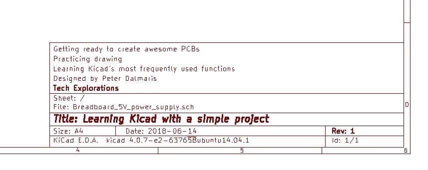
Figure 8.2: The title block filled with example text.
To edit the contents of the title block, bring up the Page Setting dialog box by clicking on File, then Page Settings (Figure 8.3).
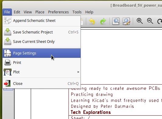
Figure 8.3: Bring up the Page Settings dialog box.
The Page Settings dialog box (Figure 8.4) contains two parts. On the left side you can control the size and orientation of the schematic page (sheet), and on the right, you can edit the information that appears in the title block.
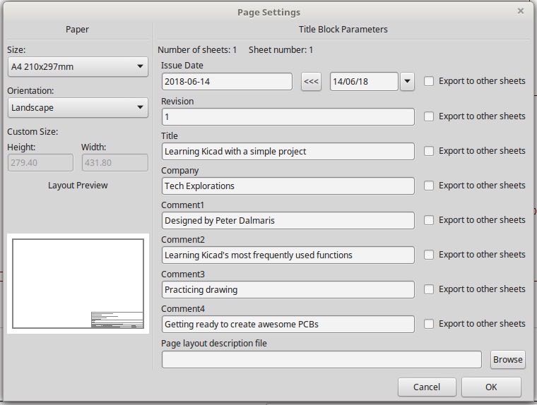
Figure 8.4: The Page Settings dialog box.
Go ahead and bring up the Page Setting dialog box. Start with setting your sheet’s size and orientation. Engineering schematics tend to be oriented in landscape. Choose the appropriate paper size for your locality.
The right side is more interesting. At the very top is the Issue Date field. You can either type a date manually or click on the '<<<' button to have today’s date copied into the field.
Continue with the rest of the fields. They are all self-explanatory. I always fill in these fields:
• Revision: Each time I make a change to my schematic, I increase the revision number by 1. Since we are starting with a new schematic, let’s use '1' as the revision.
• Title: Something sensible that describes the project without having to inspect the schematic diagram in detail.
• Comment1: The author name.
Comments 2, 3 and 4 are additional lines that you can use to provide more information about the project.
Notice that on the right side of each field is a checkbox titled 'Export to other sheets'. KiCad allows for a single schematic to be spread out to multiple sheets, as you will learn in one of the more complicated projects in Section 5. When you select one of these checkboxes, the content of the corresponding text field will be copied and displayed in the title block of all sub-sheets.
At the bottom of the window is a field titled 'Page layout description file'. This makes it possible to use a custom layout for your schematic sheets. In my normal day to day work with Eeschema I rarely have to use a layout for the sheet other than the default, but know that this is possible.
I will return to this topic shortly to show you how to customise the sheet layout.
Go ahead and fill in your own information to populate the title block in your project’s schematic sheet. Then click OK to commit the changes, and check that your text appears in the title block.
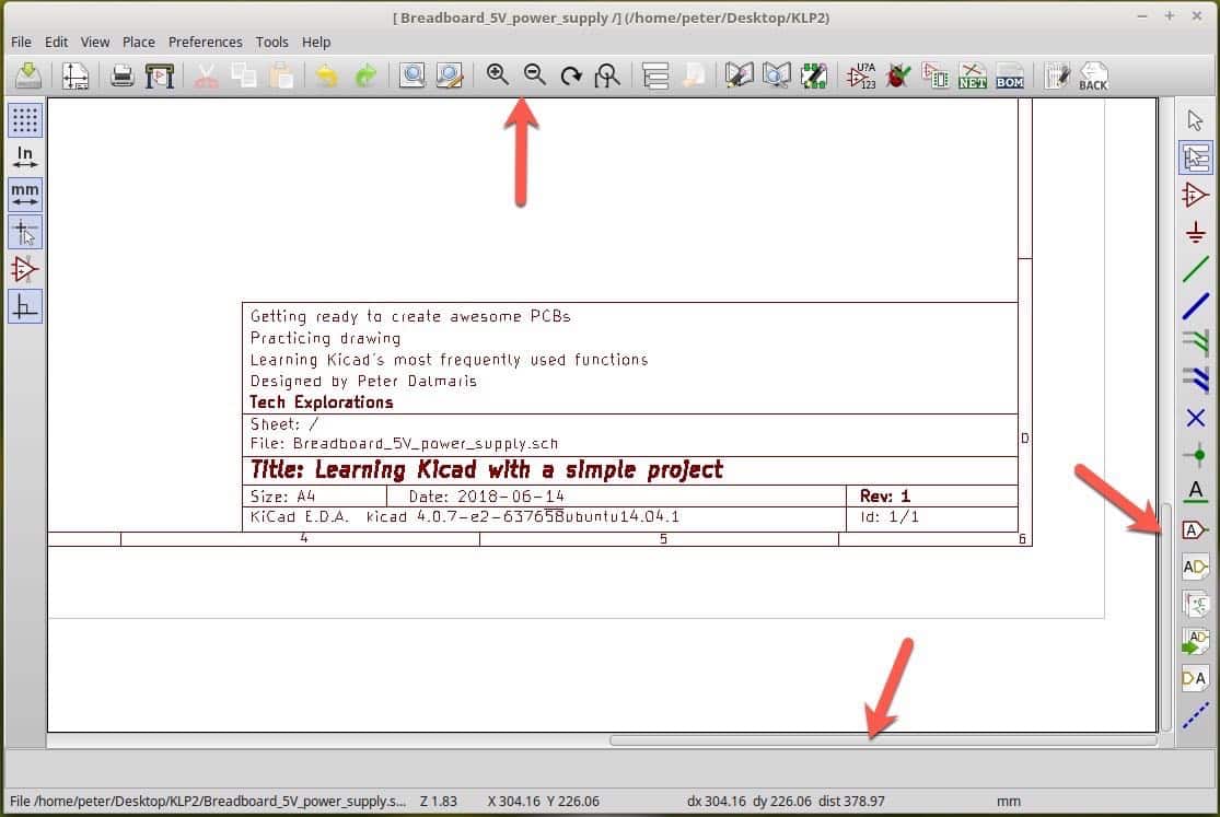
Figure 8.5: Zoom in/out and pan controls.
You can zoom in and out, and pan using the controls in the top toolbar and sheet window to reach a closer look of the title block. In the next part of this introduction, you will learn about more efficient ways to do this.
Page layout description file
Let’s return to the 'Page layout description file' that we briefly looked at earlier. Remember that this is a field at the bottom of the Page Settings dialog box (Figure 8.4) that allows you to select a sheet layout file other than the default one.
If you wish to customise the way that the page looks in Eeschema, you can do so. Please jump over to the recipe titled 'How to design a custom page layout' to learn how to do this.
Mouse buttons and hotkeys
We use the mouse and keyboard to interact with the sheet and its elements. If you have a mouse with three buttons (recommended), you can use all three to work with the symbols and the schematic on the sheet. I use a two-button mouse, with several programmable buttons (a Logitech MX Master 2S). Using my mouse configuration software, I can assign the keyboard keystrokes I use most often to the mouse programmable buttons. This can boost productivity significantly. Also important, is the scroll wheel. A scroll wheel is useful for zooming in and out of the sheet.
This table contains information about the default role of each button or button and key combinations:
Button, Keys |
Role |
Left mouse button (LMB) |
Move a selection |
Right mouse button (RMB) |
Show the context menu for selection |
Alt/Cmd + Right mouse button (RMB) |
Pan |
Scroll wheel |
Zoom in/out at the position of the cursor |
Table 8.1: Mouse controls in Eeschema.
Many other key and mouse button combinations are mentioned in the KiCad documentation; however, they will not always work as expected. This is particularly true if you have remapped your keyboard and mouse, or if you are using KiCad on a Mac, Linux PC, or inside a virtual machine.
In my experience, simple keyboard shortcuts work reliably. Try this now: with Eeschema in focus, type '?'. You should see the Hotkeys List (Figure 8.6, one of the most useful windows in KiCad (a similar Hotkeys List is available in Pcbnew). If the '?' Hotkey doesn’t work, try Ctr-F1, or click on the Help menu item and choose 'List Hotkeys…'.
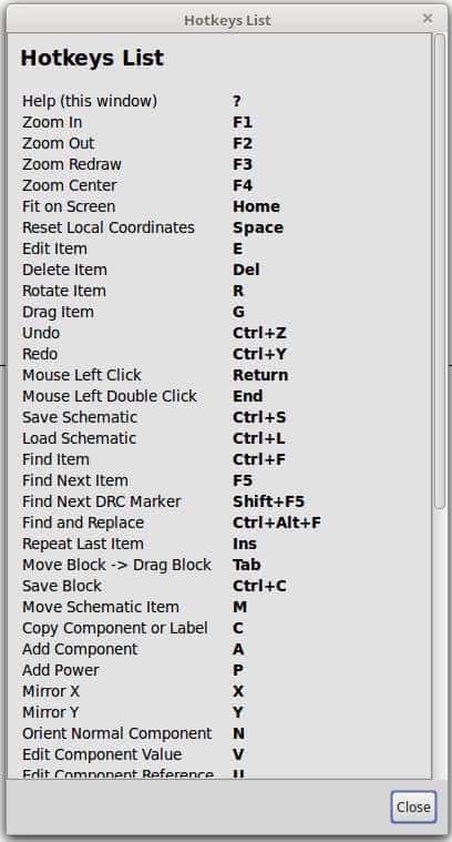
Figure 8.6: The Hotkeys List in Eeschema.
In Ubuntu Linux, which is my preferred OS for running KiCad in, you pan with the middle button. To resize the whole window, use alt-right-mouse.
There are a lot of hotkeys available, but for your quick introduction to Eeschema only a few are necessary. To use a hotkey, simply place the pointer of your mouse over a component and type the hotkey.
Hotkey |
Role |
A |
Add a new component to the sheet |
E |
Edit, reveals a dialog box where you can edit all component attributes |
R |
Rotate (each time you press 'R', the component will rotate by 90 degrees) |
G |
Drag, useful for repositioning a component without disconnecting any wires |
M |
Move. If the component has wires connected, the wires will be disconnected |
del |
Delete |
C |
Copy |
W |
Start drawing a wire |
T |
Add graphics text, useful for providing information about the schematic |
F3 |
Redraw the sheet, useful when you want to clear graphics artefacts |
Table 8.2: A list of the most frequently used hotkeys in Eeschema.
There are more hotkeys available in Eeschema, but the ones listed in Table 8.2 are the most useful ones. Before long, you will commit them to memory and use them constantly.
You may wish to change some of those hotkeys if they interfere with your existing keyboard mappings. To do this, click on the Preferences menu item, then Hotkeys, and then Edit Hotkeys (Figure 8.7).
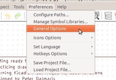
Figure 8.7: How to edit your hotkeys.
This brings up the Schematic Editor Options window. Click on the Controls tab to access the hotkeys editor (Figure 8.8):
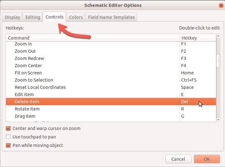
Figure 8.8: Select an existing Hotkey to highlight it, and then type in a new key or key combination.
To change a Hotkey, select it with your mouse and type in a new key or key combination.
Beware that these menus in Figures 8.7 and 8.8 may look different to your what you see in your instance of KiCad, depending on your operating system and version of KiCad.
Eeschema buttons and menus
As you can see in Figure 8.1, Eeschema provides several menu bars, as well as a status bar and the menus. Let’s look at the purpose of each one now.
Left toolbar
Menus item marked as '2' in Figure 8.1 consists of the left toolbar.

Figure 8.9: The Eeschema left toolbar.
Figure 8.9: The Eeschema left toolbar.
The buttons in the left toolbar allow you to control various visual aspects of the sheet. The button marked with '1', for example, allows you to show or hide the grid. You can further control the size of the grid via the Schematic Editor Options windows which are available through the Preferences menu item (Figure 8.10). Inspect the options in the Display and Editing tabs. In the Editing tab, you can select your preferred measurement unit (millimetres, inches etc.) among other things.
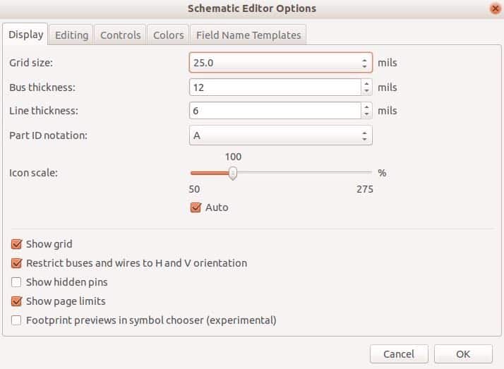
Figure 8.10: The Eeschema Preferences menu.
Depending on the grid size you have selected, you may need to zoom in before you can see the grid points. In Figure 8.11 below, you can see my 25mils grid. To be able to see it, I had to zoom in to zoom factor 3.67 using my mouse’s scroll wheel. You can see the zoom factor in the leftmost edge of the status bar, at the bottom of the Eeschema window.
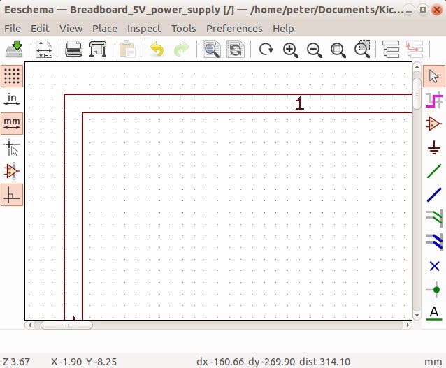
Figure 8.11: An example of my 25mils grid, at Zoom factor 3.67.
Buttons marked 2 and 3 in Figure 8.1 allow you to select your preferred length unit. You can select between inches (button 2) and millimetres (button 3).
Button 4 allows you to select the shape of the cursor. There are two options: small crosshairs, or long crosshairs (Figure 8.12). I find that long crosshairs are useful when you work on large and spread-out schematics. The XY lines extend across the full height and length of the sheet so that you can easily determine if the position of the cursor is aligned with the position of other components in the schematic.
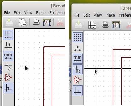
Figure 8.12: Short (left) and long (right) crosshairs.
Button 5 in Figure 8.1 allows you to show or hide normally invisible pins in integrated circuit schematic components. Such components are often designed to not show certain pins, such as power or ground, in order to reduce visual clutter. KiCad can automatically connect these hidden pins to the appropriate power sources if certain conditions apply.
Finally, Button 6 in Figure 8.1 allows you to lock the orientation of wires to 90 degrees when it is enabled. You can see an example of what this button does in Figure 8.13. The left green wire is restricted to 90 degrees orientation (button 6 was pressed), while the green wire on the right is not restricted.
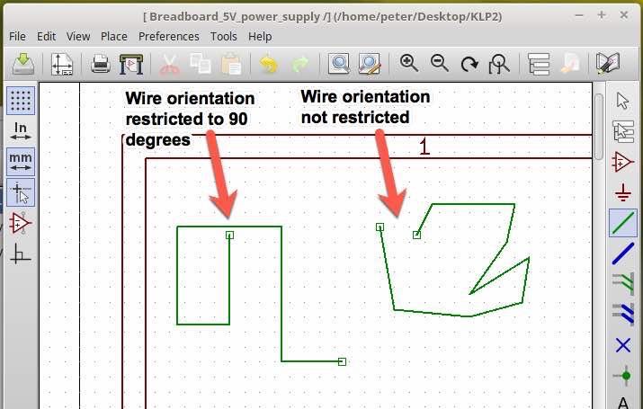
Figure 8.13: You can restrict wire orientation to 90 degrees, or leave it unrestricted.
You can experiment with the wire function too. Place your mouse pointer inside the sheet, and type 'W' to enable wiring mode. Move your cursor and click, then repeat to define the first segment of the wire. Continue for a few more segments. When you are finished, double click to end drawing the wire, or type the escape key to exit wiring mode. By using the Escape key, you actually cancel the drawing process, and the wire that you draw will disappear. Click on the orientation button to change orientation mode, and create a few more wire segments. Can you see the difference between the two modes?
I find that schematic diagrams look much better and are more readable when wire orientation is restricted to 90 degrees, so I do almost all my wiring that way.
Right toolbar
The right toolbar includes tools that allow you to add the various elements that make up a schematic, including symbols, wires, labels, and text. This toolbar also contains functions useful in manipulating sub-sheets.
You can see the right toolbar in Figure 8.14. In the following paragraphs, you will become familiar with the buttons you will need in this introductory project, such as the component and power symbol selectors, wires, and delete. We'll leave the rest (like the bus and entry points tool, global labels tool and the hierarchy navigation tool) for more complicated projects in Section 4.

Figure 8.14: The right toolbar allows you to control the various elements that appear on the sheet, and sub-sheets.
When you click on the button labeled ‘1’, you will get you out of whichever other command or tool you are using. For example, if you are working on creating wires using the wire tool (item 5 in the right toolbar), you can either type the ESC key or click on button 1 to exit the wire tool.
I often forget about the toolbar and instead use the hotkeys to switch from one tool to another, and the ESC key to reset the cursor. As I mentioned previously, hotkeys will become committed to your muscle memory and help you speed up your work with KiCad. Until then, let’s continue with understanding the most important buttons in the right toolbar.
Component selector
Button 3 allows you to select a component from the library and drop this component onto the sheet. There are two ways to access the component chooser:
- Click on button 3 to choose the component chooser tool, and then click on the sheet on the location where you would like to drop the component,
- Or, place the cursor somewhere on the sheet where you would like to drop the component and then type ‘A’ (for ‘Add’).
Either way, the dialogue box in Figure 8.15 will appear.
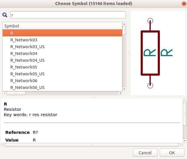
Figure 8.15: The component chooser.
To find a component, you can type its name in the filter box (top of the window), or browse through the libraries. In Figure 8.15 I typed ‘r’ in the filter as I was looking for a resistor. The resistor component appears first in the list of results, followed by other components that have a name that begins with ‘R’. To drop the component to the sheet, click on it to select it and then click the ‘OK’ button.
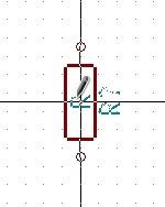
Figure 8.16: When you close the component chooser, the component is attached to the cursor.
When you close the component chooser, the component is attached to the cursor. You can move your mouse around and you will see how the component moves with it. You can also use the ‘R’ hotkey to rotate the component to the orientation that you need. When you have placed the component on the correct location and orientation, simply click to commit it in place. The component will then have a solid outline and label, and will no longer be attached to the cursor.
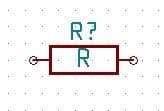
Figure 8.17: When you commit a component to the sheet, it’s outline becomes solid.
If you want to move it again, place the cursor on it and type ‘M’ (for ‘Move’). The component will become attached to the mouse and you will be able to move it until you commit to a new location with another click.
Power port selector
Button 4 in the right toolbar allows you to select and place a power port. A power port is a symbol that represents a power connection, such as a 5V voltage source or a ground (GND). You can find and select a power port using the normal component selector tool (button 3 in Figure 8.14). After all, a power port is just another symbol. The power port button simply provides a shortcut to this particular kind of symbol. Clicking on the power port button will bring up the same symbol chooser window that is depicted in Figure 8.15, except that now the filter takes us straight to the power-related components, saving us a bit of time.
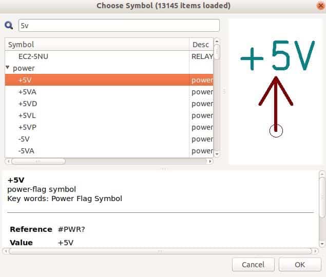
Figure 8.18: The power component chooser.
In Figure 8.18 I have also used the filter to find a 5V power source. Clicking the 'OK' button will add this component to the sheet. I now have 2 components in my sheet, as you can see in Figure 8.19:
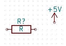
Figure 8.19: Two components are now in the schematic sheet.
Because the next tool you will learn about is the wire tool, let’s add two more components to our sheet: a GND power component, and an LED. After that, we will use the wire tool to connect them. 8.20 shows my current schematic. Try to make yours look as similar as you can do this by adding the two new components and using the ‘R’ and ‘M’ hotkeys to rotate and move them to their correct positions.
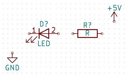
Figure 8.20: Four components are now in the schematic sheet.
Wiring and delete tools
Now that we have these four components in our sheet, let’s wire them. To do this, we’ll use the Wire tool, which is labeled as ‘5’ in Figure 8.14. To enable wiring mode, click on the wiring button or type ‘W’ (for ‘Wire’).
If you typed 'W' then your cursor is already drawing a new wire on the sheet. Move your cursor around and you will see the green wire segment following the cursor. Most likely, the beginning of the wire will not be within one of the circles that indicate a pin on a component. It is unlikely that you want to create a ‘floating’ wire (I.e. a wire that is not connected to something), so hit the ESC key to stop drawing the wire. The wire tool is still enabled (you can confirm that by looking at the state of the wire button in the right toolbar).
Let’s try again to draw the first wire. We’ll make this wire connect the GND component and the cathode of the LED component. Use the scroll wheel of your mouse to zoom in to the pin that is coming out of the GND symbol, and pan the sheet so that you can comfortably see both GND and LED components.
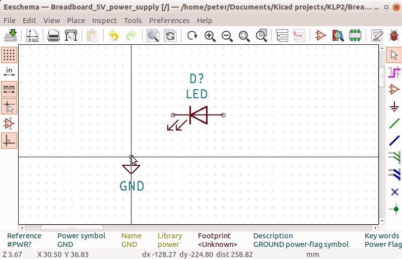
Figure 8.21: To connect a wire to a pin, place the cursor in the middle of the pin circle.
With your cursor right in the middle of the circle at the edge of the pin, and with the wire tool selected, click and release. You now have the start of the first wire segment.
Move the cursor to the centre of the circle that marks the edge of the cathode pin of the LED component. Assuming that you have turned off the wire orientation restrictions, you will now have a wire that connects the GND and LED in one straight line, like in Figure Figure 8.22:
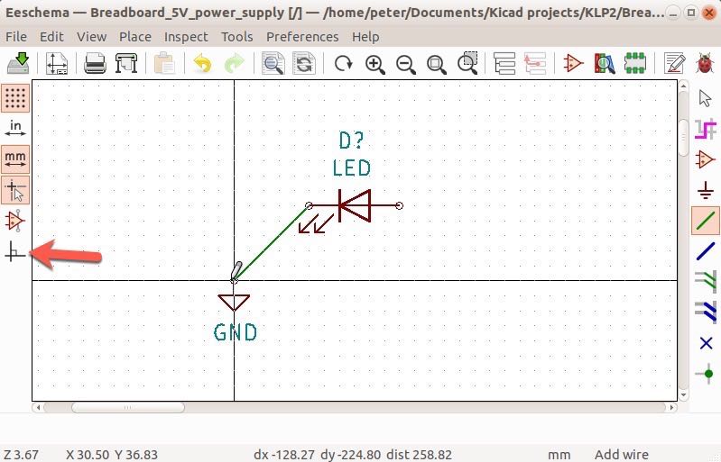
Figure 8.22: GND and LED are connected with a straight wire. Notice that orientation restrictions are off.
I prefer my wires drawn using horizontal and vertical lines, so let’s try again. First, delete the existing wire by selecting the delete tool (marked as ’20’ in Figure 8.14). Then, click on the green wire to delete it. If your grid is large, you may not be able to get your cursor right on the line, and your clicks will have no effect. You can either change the grid size to something finer or click on the wire on a location where a grid dot and the wire touch.
Once you delete the wire, type ‘W’, click on the orientation button in the right toolbar to enable it, and try again to connect the GND and LED components. Just like the first time, click on the circle of the GND component, then click again on the circle of the LED’s cathode pin. You should have something like this in your sheet:
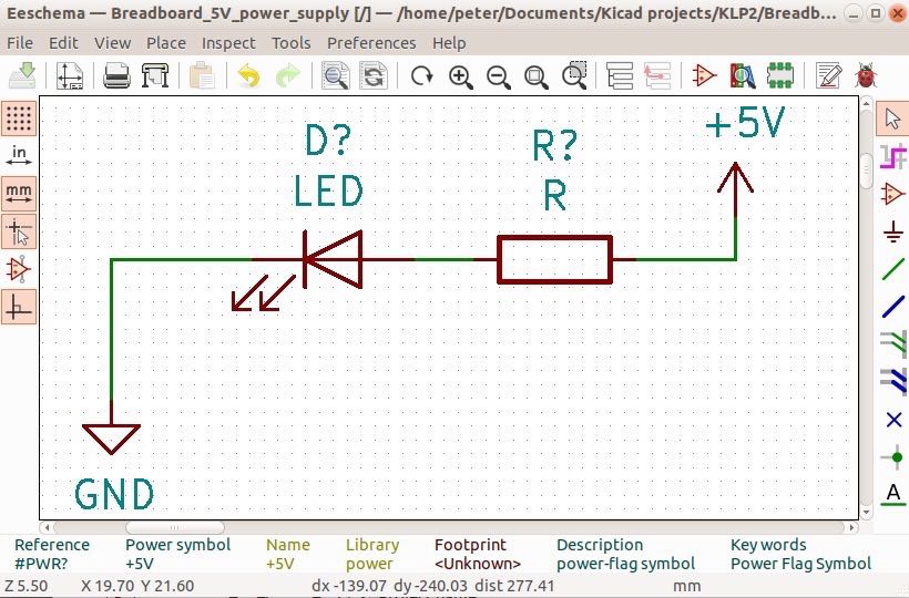
Figure 8.24: The final schematic of a simple circuit with four components.
Junction tool
The next one of the buttons that you will need for the first project is labeled ’10’ in Figure 8.14. This is the 'junction' button.
With the junction button, you can create connections between wires. Let’s have a look at a simple example.
Go ahead and create two wires that intersect each other, like the example in Figure 8.25. To end drawing a wire in mid-air (not connecting the wire to a pin), double-click.
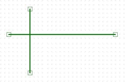
Figure 8.25: two wires intersecting but not connected (there is no junction).
These two wires may look like they are connected because the intersect, but they are not. There is no electrical connection between them. To connect them electrically, use the junction button (labelled ’10’ in Figure 8.14 or indicated by the arrow in Figure 8.26).
Try that now. Click on the junction button to enable it, and then click on the exact location where the two wires intersect. In Figure 8.26 you can see that a large green dot marks the exact location where the two wires are electrically connected. Also, notice that the junction button is pressed.
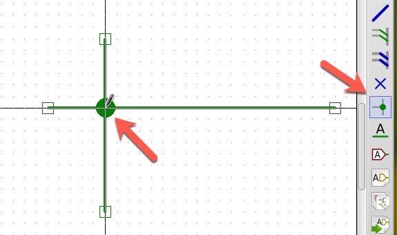
Figure 8.26: The two wires are electrically connected as indicated by the large green dot, that junction symbol.
You can also connect two wires by drawing the end of one onto any part of an existing wire.
Try this: use the ‘W’ hotkey to get back into wiring mode, start a new wire, and click on any part of an existing wire to end the drawing. Notice that a junction dot is added to confirm that the two wires are now electrically connected, not simply intersecting each other. Your schematic should look like the one in Figure 8.27.
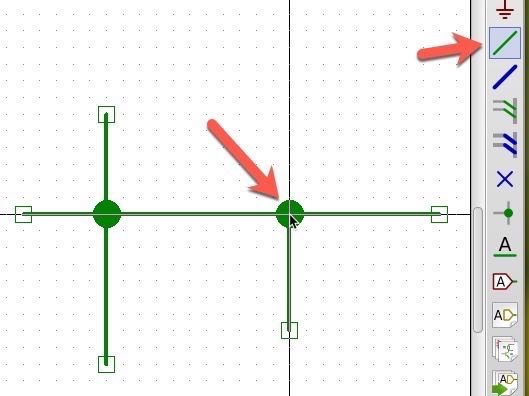
Figure 8.27: You can connect two wires by drawing the end of one into another.
You now have a completed circuit schematic, created using only 5 of the buttons in the right toolbar. That is enough to allow you to create your very first PCB, which is what you will do later in this section. You will learn about the rest of the buttons in the right toolbar later in this book, starting in Section 4.
Let’s continue with the most important functions in the right toolbar.
Text tool
The last two of the buttons that you will use in this introductory project are the Text button and the Graphics Line button. These do exactly what their names suggests.
Using text and simple line graphics in your schematic have the potential to increase readability, especially in a large and complicated project.
Let’s start with the Text tool. Click on the text button (labeled ’18’ in Figure 8.14), then click somewhere close to the LED in the schematic that you started earlier in this section. You will see the the text properties window, as in Figure 8.28.
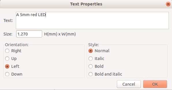
Figure 8.28: the Text Properties window allows you to insert free text in your schematic.
Type in something sensible to provide useful information that will assist the reader. I’d like my circuit to use a 5mm red LED, so that is what I typed in the Text field. I also like the text to appear in a small size font, so I entered ‘1.00’ in the Size field. I left the rest of the widgets unchanged, but feel free to experiment with them and see what they do.
When you click ‘OK’, the new text will be attached to your mouse pointer so that you can position it at the exact location you want. The text appears faded as you move it around, like in Figure 8.29.
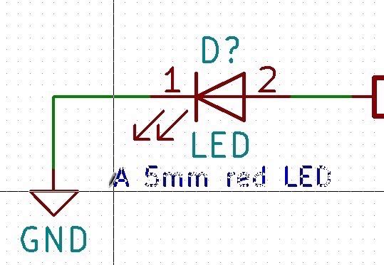
Figure 8.29: When you exit the Text Properties window, the new text is attached to the mouse pointer so you can position it.
When you have the new text in position, right-click your mouse to commit it. The text will look solid, as in Figure 8.30.
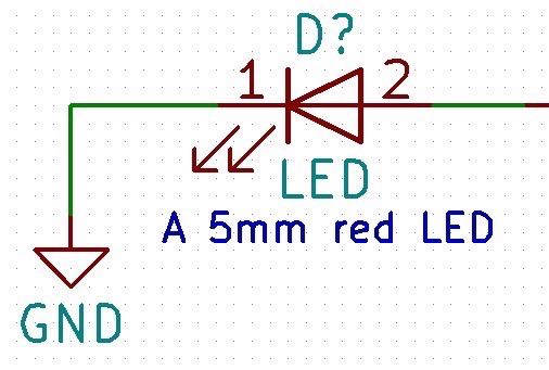
Figure 8.30: The new text is committed to the sheet.
You can use the text tool by using the ’T’ hotkey (for ‘Text’). Place your cursor on the position where you would like to place the text and type ’T’. The same dialog box that you saw in Figure 8.14 will appear, and from there onward the process is the same as if you had clicked on the Text button.
If you make an error in the text, you can easily fix it by placing your mouse over the text and typing ‘E’ (for ‘Edit’). Again, the Text Properties dialog you saw in Figure 8.14 will appear, and any changes in the text or its properties will appear when you click on the ‘OK’ button.
The ‘E’ hotkey works with any other components in the sheet, not just text. Go ahead and try it on the LED and resistor components, and see what happens.
Try adding one more text item to provide additional information about the resistor. For example, add text the says ‘current limiting resistor’, so you end up with this result (Figure 8.31):
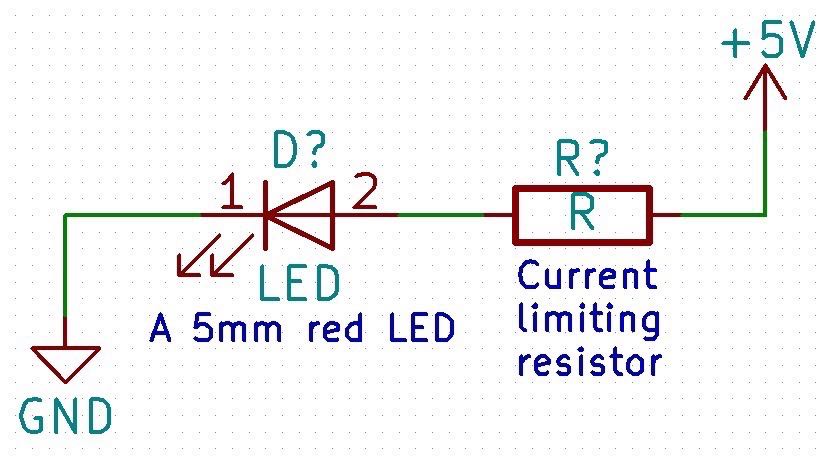
Figure 8.31: More text, this time in three lines.
Notice how the text ‘Current limiting resistor’ appears in three lines instead of one? You can do this simply by inserting a carriage return after each word, or after a word where you would like the line to end (Figure 8.32).
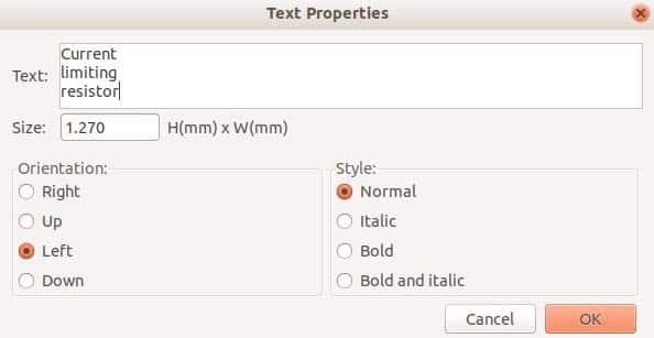
Figure 8.32: You can spread text over multiple lines.
In Figure 8.32, I spread the text over three lines, as you can see in the Text text field.
One more thing before we look at the graphics line and polygon tool: To move any component or schematic element to a new position, use the ‘M’ hotkey (for ‘Move’). Try it now: place your mouse cursor over the text ‘Current limiting resistor’. The text is now attached to the cursor. Move your cursor with the attached text to a new position, then click to commit.
I remind you that you can use the ‘M’ hotkey on any component, not just text. However, if the component that you are moving has wire connections, these will be broken, and you will have to rewire it manually. To move a component without breaking its wiring, you can use the ‘G’ hotkey (for ‘Grab’).
Play with the ‘M’ and ‘G’ hotkeys until you feel confident that you understand them, and then move to the next part where you will learn about the Graphics line and polygon tool.
Graphics line tool
The last of the buttons in the right toolbar that you will need for this introductory project is the Graphics Line of Polygon button. It is the fourth one from the bottom, labeled ’17’ in Figure 8.14.
By clicking on the button you will be able to draw straight lines. You can draw multiple straight lines and create boxes or other polygons. You can use these lines of polygons to do things such as group parts of your schematic together, put boxes around text or simply highlight text, or add some simple graphical elements to your schematic in order to improve its readability and make it more aesthetically pleasing. You can also enable this tool by using the ‘i’ hotkey.
Let’s make a box to enclose our small circuit. Place your mouse around the bottom left edge of the circuit (or anywhere else where you would like the box edges to exist), and type ‘I’. Draw the box by moving your mouse to the next corner and left-clicking to mark the end of that segment. To finish drawing, double left-click. You should have something like the example in Figure 8.33.
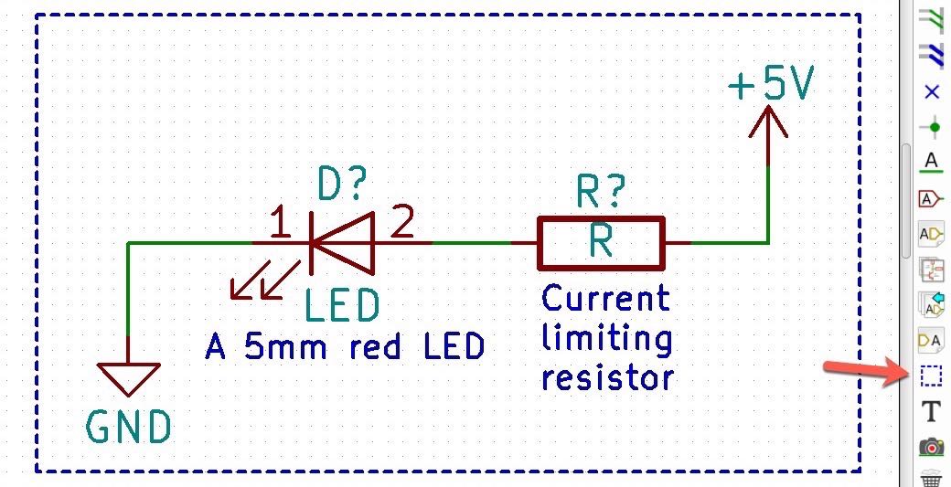
Figure 8.33: Use the Line tool to draw lines and polygons.
The line tool is very basic. You can change its color, thickness, or pattern. The only kind of line you can draw is what you see in the example of Figure 8.33.
If you make a mistake, you will need to use the Delete tool and click on each segment that you want to delete, then re-draw. The ‘E’ and ‘G’ hotkeys also work on lines.
Top toolbar
The top toolbar includes collections of buttons that perform a variety of functions. There are buttons for saving your schematic diagram to disk, printing it to paper or in other file formats, zooming in and out of the sheet, checking the correctness of the schematic, and more.
In this chapter, you will become familiar with the top toolbar and learn how to use the functions you will need for this first project. Figure 8.34 depicts this toolbar, annotated with numbers for easy reference.

Figure 8.34: The top toolbar allows you to save and print your sheet, as well as perform many other functions.
Quick tour of the top toolbar
Let’s have a quick look at the functions available through the top bar before we concentrate on those that are useful for this first project. Table 8.3 (below) describes the functionalities that you can access through the top-bar buttons.
Button |
Description |
1 |
Saves the file to disk (you can also type Ctr-S to achieve the same result, or click on File and then 'Save Schematic Project'). |
2 |
Configure the page settings. You have already learned about this in the segment titled '8.1. The schematic sheet'. |
3 |
Print the sheet to paper. |
4 |
Export the sheet to various file formats like PDF, PostScript, SVG, DXF and HPGL. |
5 |
Paste a copied item |
6 |
Undo and redo the last command. |
7 |
Find and replace text in the sheet |
8 |
Redraw (useful when the sheet graphics rendering leave artefacts behind) |
9 |
Zoom in and out |
10 |
The left button in this group will change the zoom factor so that the schematic fits in the window. The right button, when enabled, allows you define a rectangle with your mouse, and zoom in to the contents enclosed in the rectangle. |
11 |
Navigate through hierarchical sheets |
12 |
Access the library editor, which allows you to create or edit symbols |
13 |
Access the library browser so that you can find a symbol and edit to your schematic |
14 |
Access the footprint editor. With the footprint editor, you can create new footprints or modify existing footprints. |
15 |
Annotate the schematic components so that each component has a unique identifier |
16 |
Perform the electrical rules check (ERC). This check detects errors such as unconnected wires. |
17 |
Associate symbols and footprints. This will trigger the Cvpcb application. |
18 |
Generate the Netlist file. This file is then imported into Pcbnew so that you can continue the process with the board layout. |
19 |
Symbol field editor. In this editor, you can edit the symbol fields in bulk, instead of doing so individual for each symbol in the symbol’s properties window. |
20 |
Create a Bill of Materials. This uses a plugin that can read the contents of the schematic sheet and generate a spreadsheet that contains a list of its components. |
21 |
Start Pcbnew. Using Pcbnew, you can create the board layout. |
22 |
Back-import component footprints (selected using CvPcb) into the 'footprint' fields. |
Table 8.3: The functions that are available through the top toolbar.
Of the functions you can see in Table 8.3, the ones you will need in this project are 1, 2, 8, 13, 15, 16, 17, 18 and 20.
I’d like to concentrate on functions 13 (library browser), 15 (annotator), 16 (ERC), 17 (associator) and 18 (Netlist) since the rest are self-explanatory or you already know how to use them (1, 2, 8).
Library browser
Click on button 13 to bring up the Library Browser. It should look like the example in Figure 8.35.
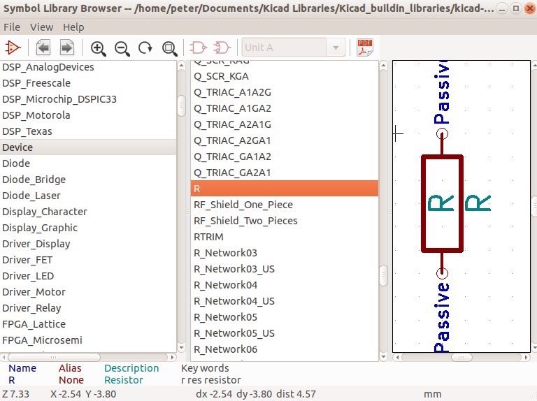
Figure 8.35: The symbol browser allows you to inspect the available symbols.
Using the library browser, you can find a symbol among the available symbol libraries. The symbol library browser is just that, a browser. It is useful for browsing through and editing the available libraries and symbols. When you find a symbol you want to use, you can insert it in your schematic; use the 'Place symbol' button from the right toolbar or the 'A' key for that.
The browser consists of three panes. The left-most pane contains the libraries. The middle pane contains the symbols that are part of the selected library. And the right pane shows the selected symbol.
You can resize the panes by placing your mouse over one of the vertical dividing lines, then dragging the line to the left or right using your left mouse button.
Try this out: in the left pane, scroll up and down to become familiar with the available libraries. Find the one named 'device', and click on it. Did you notice that the contents of the middle pane were updated as soon as you selected the device library? Now scroll up and down the middle pane and look for the symbol named 'R'. This is the standard resistor symbol. Click on it and see how the graphical representation of this symbol appears in the right pane.
You can use the scroll wheel in the right-most pane to change the size of the symbol, but please note that this won’t change its size on your schematic; it only affects the symbol size in the library browser.
To quickly browse through the available symbols, you can use the filter. Try this now: Select the symbol library browser from the top toolbar, and then click on the Filter button (at the start of the arrow in Figure 8.36).
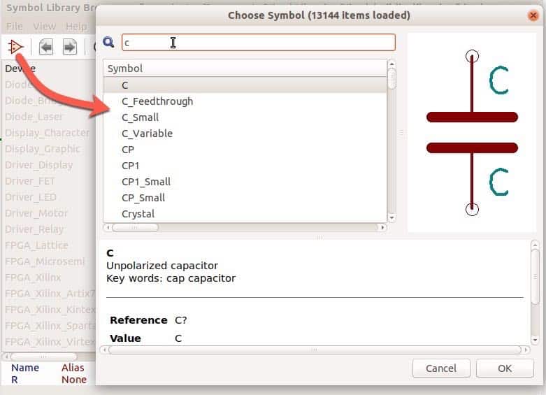
Figure 8.36: The symbols browser filter allows you to quickly find a symbol.
The filter window will come up, where you can add text in the filter text field. In the example in Figure 8.36, I typed 'C' as I was looking for a standard capacitor. Once you make your selection, double left-click on it or click Ok, to have the symbol’s graphical symbol appear in the browser’s right pane.
The annotator
Annotating your schematic is a required step of the PCB design process. To annotate your schematic, use the Annotator tool, which is accessible by clicking on button 15 in Figure 8.34.
Let’s return to our tiny schematic, that consists of a resistor and an LED. Here it is again, in Figure 8.37:
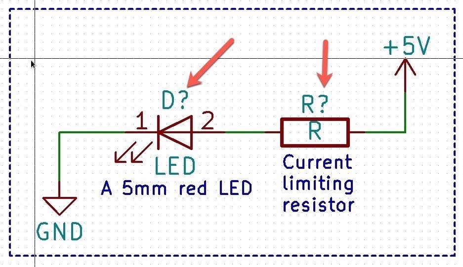
Figure 8.37: In this schematic, the diode and resistor symbols do not yet have a unique identifier.
In this schematic, notice that the diode and resistor symbols do not have a unique identifier. The arrows point to the question marks next to the 'D' and 'R' symbols, that indicate that the schematic has not been annotated yet.
To do the annotation, click on the annotator button (15 in Figure 8.34). This will bring up a new window that is titled 'Annotate Schematic', that you can see in 8.38.
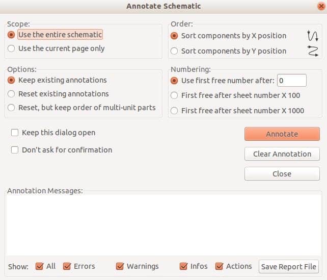
Figure 8.38: This dialog box allows you to control the annotator.
The annotator dialog box allows you to control how the annotator will complete its task. For example, if your schematic spans across multiple sheets, you can choose to annotate all of the sheets or only the current one. If you have annotated the schematic in the past and added new symbols which are not annotated, you can also choose to retain existing annotations and only annotate the new symbols. You can also control the direction of annotation, and the numbering system.
Let’s keep things simple, and accept all the defaults. Click on the Annotate button, and accept the warning dialog box that may pop-up. This will complete the annotation, and update your schematic. Click on the Close button to close the dialog. The result should look like the example in Figure 8.39:
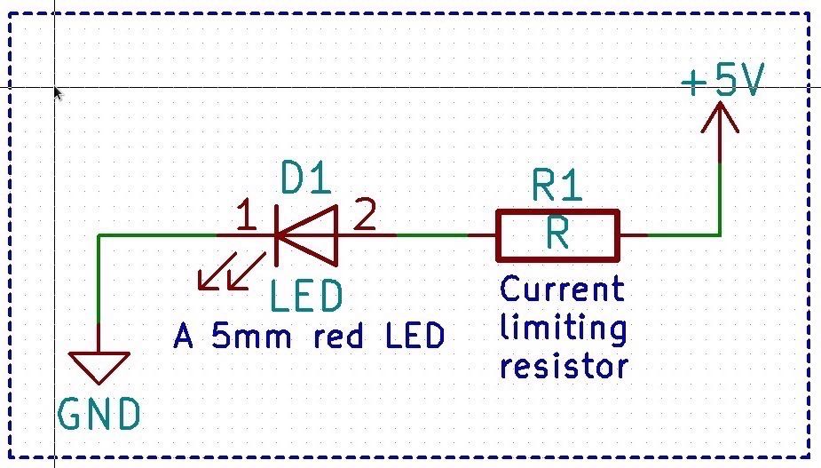
Figure 8.39: The symbols now have a unique identifier.
Let’s continue with the electrical rules check (ERC).
Electrical rules check (ERC)
Our simple schematic diagram looks correct, from an electrical point of view. All wires seem to be correctly connected. The power ports also look correctly connected.
Not much can go wrong in a small schematic like the one we are currently working on. But as you start working on larger and more complicated circuits (as we will be doing very soon), the risk of errors will increase.
It is critical that we can identify and correct any errors before we continue our work with the PCB layout editor (Pcbnew), and this is the purpose of the Electrical Rules Check (ERC) function.
Let’s go ahead and try this now, in our simply LED and resistor circuit.
Click on the ERC button (labeled 16 in Figure 8.34). This will bring up the ERC dialog box, which is empty (Figure 40).
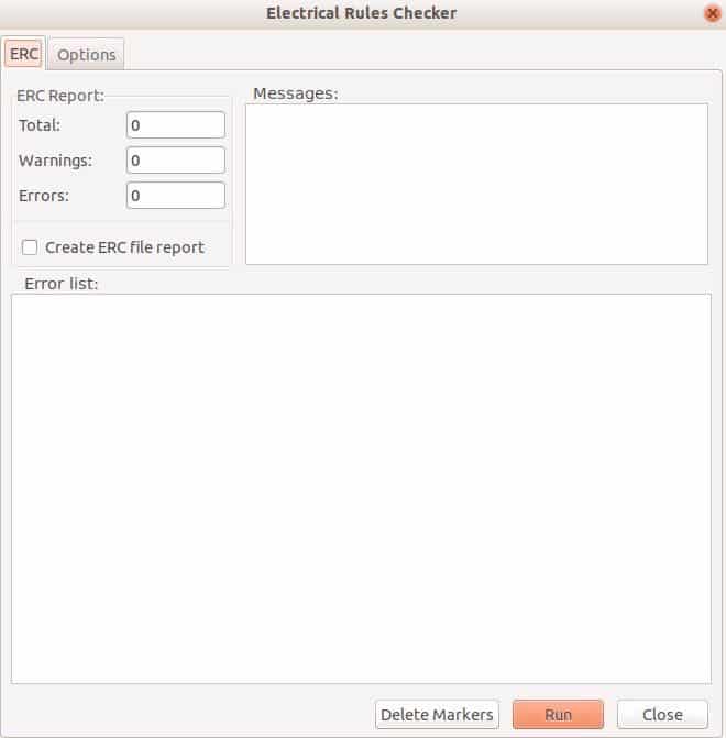
Figure 8.40: Starting the Electrical Rules Checker.
To start the check, click on the Run button. The ERC will do its work, and produce a list of errors if any. In my case, it did produce two errors, as you can see in Figure 8.41:
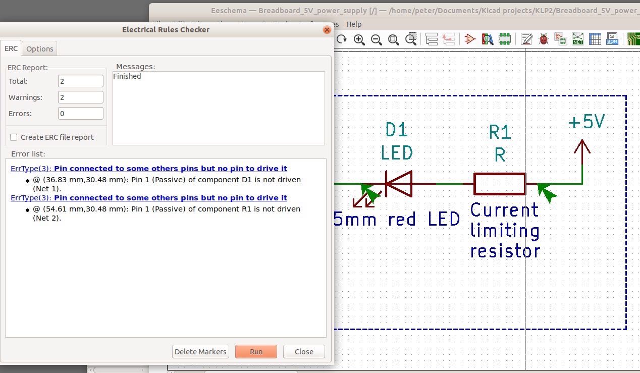
Figure 8.41: Even in such a simple circuit, errors are lurking!
The checker returned two instances of the same error:
ErrType(3): Pin connected to some others pins but no pin to drive it
To help us find and fix the error, it also marked the location of the errors in the schematic using green arrows. This is probably one of the most frequent errors that I encounter in KiCad. The error message itself may not make much sense, but it is straight-forward. KiCad is complaining that there is no power source for the circuit. It 'knows' that every circuit needs a power source to operate, and that in the case of this circuit, it can’t find one.
Even though we do have a 5V and a GND symbol, these have to be explicitly marked as power sources to satisfy the ERC rules. While not intuitive for people new to PCB design, it will make sense if you think about. In general, a circuit contains wires that convey signals (like the voltage that comes from an analog sensor) and power (like the current that comes from a battery). KiCad needs to be able to tell the two apart, and it is our responsibility as designers to mark our schematic explicitly.
Let’s go ahead and fix ERC’s errors by marking the wires that are coming out of the 5V and GND symbols as power wires. Going forward, I will also be using the word 'net' to mean a wire. The word net is used extensively in KiCad, and it is good at this point to start becoming used to it.
Let’s go to the schematic, place the cursor near the 5V symbol and type the 'A' key so we can add a new symbol. The symbol chooser will appear (Figure 8.42). Type 'pwr' in the filter to get to what we are looking for faster. The PWR_FLAG symbol is in the 'power' library.
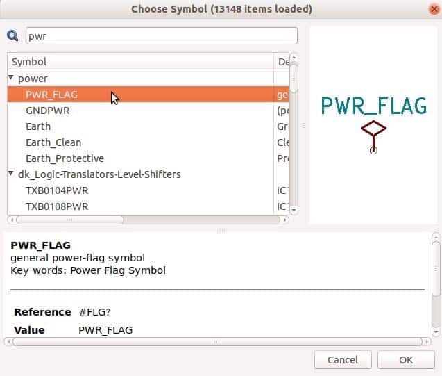
Figure 8.42: The power flag (PWR_FLAG) symbol.
Click 'OK' to add the PWR_FLAG symbol to the schematic. Position it close to the 5V symbol, and connect it to the net that connects the resistor and the 5V symbols. You should now have something like the example in Figure 8.43.
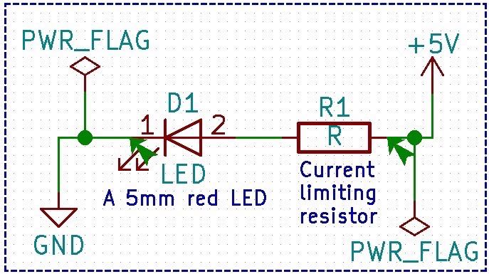
Figure 8.43: With the PWR_FLAG symbols we can mark nets explicitly as power nets.
What we have now is a circuit with the exact same symbols as before (an LED, a resistor, and the GND and 5V symbols). But now, we have explicitly told KiCad that the nets between the LED and GND, and resistor and 5V convey power. The PWR_FLAG symbols are not 'real', in the sense that they do not have a footprint that will appear in our PCB. Think of them as tags, or instructions for providing KiCad with the information it needs to operate.
Connecting the PWR_FLAG symbols to the two nets with the error messages should fix those errors. Let’s verify. Run the ERC again by clicking on the ERC button (labeled 16 in Figure 8.34), and then on 'Run'. Both errors should be cleared, and there should be no green arrows in the schematic. Your schematic should look like the example in Figure 8.44:
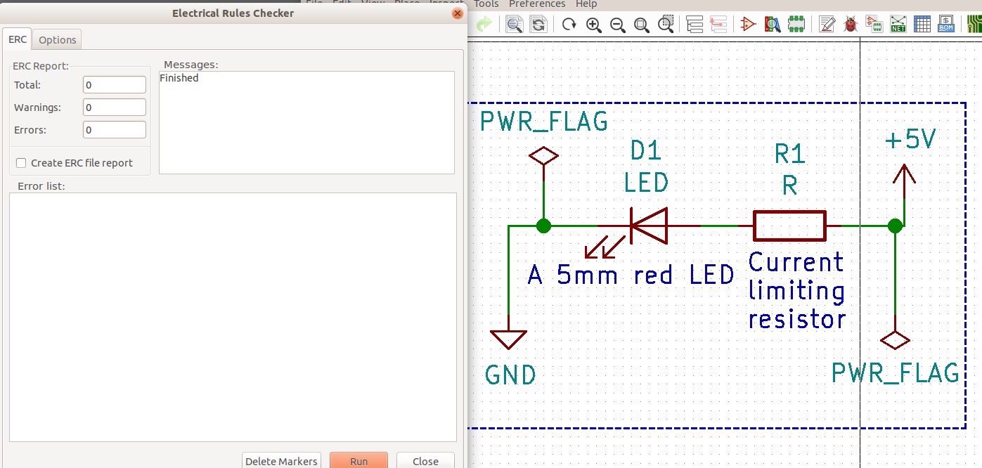
Figure 8.44: Thanks to the PWR_FLAG symbols the ERC errors are cleared.
Now that this simple schematic is electrically correct, we can continue by associating the schematic symbols (the D1 and R1 symbols that you see in Figure 8.44, with the footprints that we will work within the layout editor (Pcbnew).
Cvpcb: Associate components and footprints
KiCad’s approach to PCB design is to recognise that a PCB starts its 'life' as a schematic diagram. In the schematic, abstract symbols represent the components that will eventually populate the PCB. But, the keyword here is 'abstract'. A simple resistor symbol in the schematic can be implemented as one specific physical resistor out of many possible ones.
You can choose to use a surface mount resistor, that come in a variety of sizes and packages: 0201, 0402, 0603, 0805, and so on. You may choose a through-hole resistor, which also comes in a variety of sizes and packages: 3mm, 6.5mm, 8.5mm and so on.
KiCad’s designers decided that it makes sense to separate the schematic symbols from the footprints and give maximum flexibility to us, the PCB designers, to assign a footprint to a symbol. Once you get used to this idea, you will appreciate the power of this approach. You will be able to create a single schematic, and from it derive multiple PCB layouts. For example, you can create a through-hole component version of the PCB during the prototyping stage to make sure that your PCB works, and then create a surface-mounted version of the PCB which is better for assembly using pick-and-place machines.
The tool that connects the schematic symbols with the footprints is Cvpcb. Let’s use it now.
Click on the Cvpcb button (marked as '17' in Figure 8.34). In Figure 8.45 you can see Cvpcb before we make any associations.
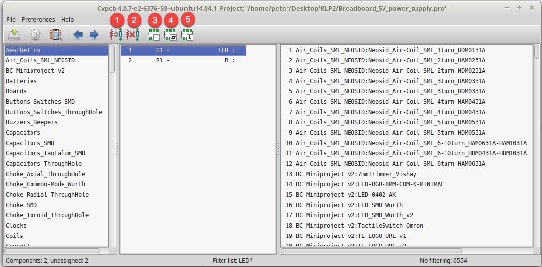
Figure 8.45: Cvpcb before we make any associations.
The tool contains three parts. In the Left pane are the footprint libraries. These libraries contain footprints. We will search in them to find appropriate footprints for the resistor and LED. In the middle pane is the list of schematic symbols and their associated footprints. At the moment, there are no associations.
Let’s start by creating an association for the LED, which is already selected in Figure 8.45. By default, the first library in the left pane is selected, and a long list of items showing in the right pane. Cvpcb provides search filters in the form of the buttons 3, 4 and 5 in Figure 8.45. If none of the filters are selected, then in the right pane you will see all of the footprints that are included in all of the libraries. This is a very long list to search through even if you are only using the default footprints that come with KiCad. Click on any other library in the left pane, and you will notice that the list in the right pane doesn’t change. It still contains everything.
Try out the Library filter, that is labeled as '5', and you can also easily recognise thanks to the 'L' in its button icon. This filter allows you to display in the right pane only those footprints that belong to the selected library in the left pane. Click on the Library filter button to enable it, and then try out a few libraries. See how the contents of the right pane change as you switch through libraries?
The button labeled as '4' is another filter that narrows down the items you see in the right pane based on the number of pins that the selected device in the middle pane has. For example, in Figure 8.45 the selected device has two pins. When you enable the 'number of pins' filter, only footprints with two pins will appear in the right pane.
Finally, the button labeled as '3' is the keyword filter. It narrows down the items you see in the right pane to only those that contain a keyword that matches that of the selected item in the middle pane. Click on it to select it. Unless you have selected the LEDs library in the left pane, the right pane should be empty, because the random library you have selected does not contain any items with the keyword 'LED' in its name.
With all three filters selected, use the scroller of the left pane to find a library named 'LEDs'. In the right pane, you will see all of the available matching footprints (Figure 8.46).
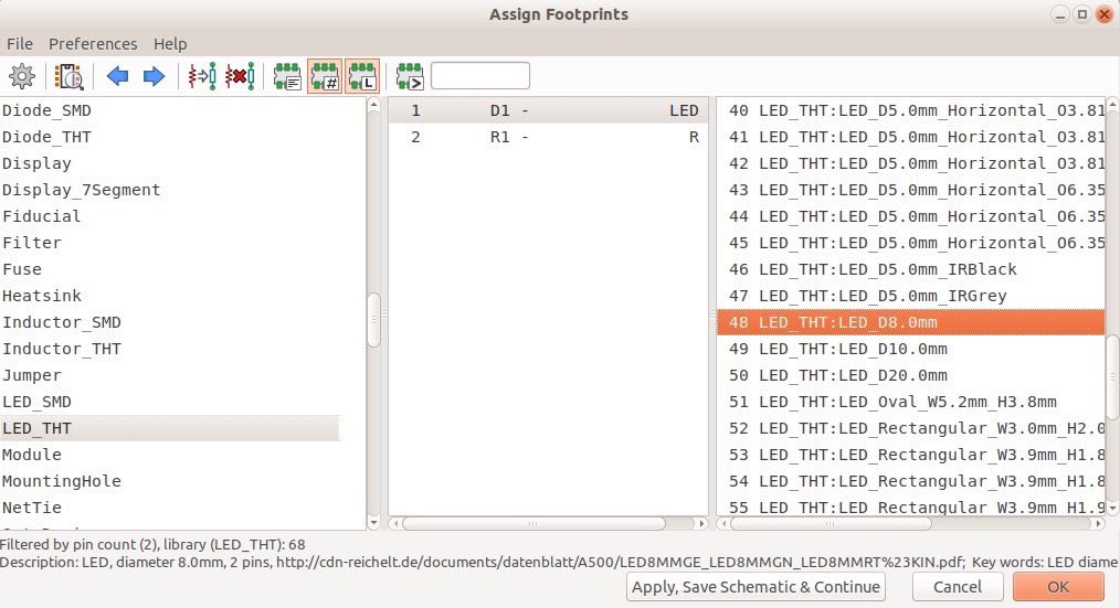
Figure 8.46: Finding the right footprint for the LED schematic symbol.
There are a lot of options. You can associate the LED symbol with a Surface-Mounted Device (SMD) or Through-hole (TH) component of various sizes and orientations. I am not too concerned about which one I will select in this example since we are only warming up, and will not actually manufacture this PCB. Select a reasonable footprint, like the one I have in Figure 8.46, which is an 8mm LED.
You can see the footprint by clicking on the Footprint button, as in the example in Figure 8.47 .
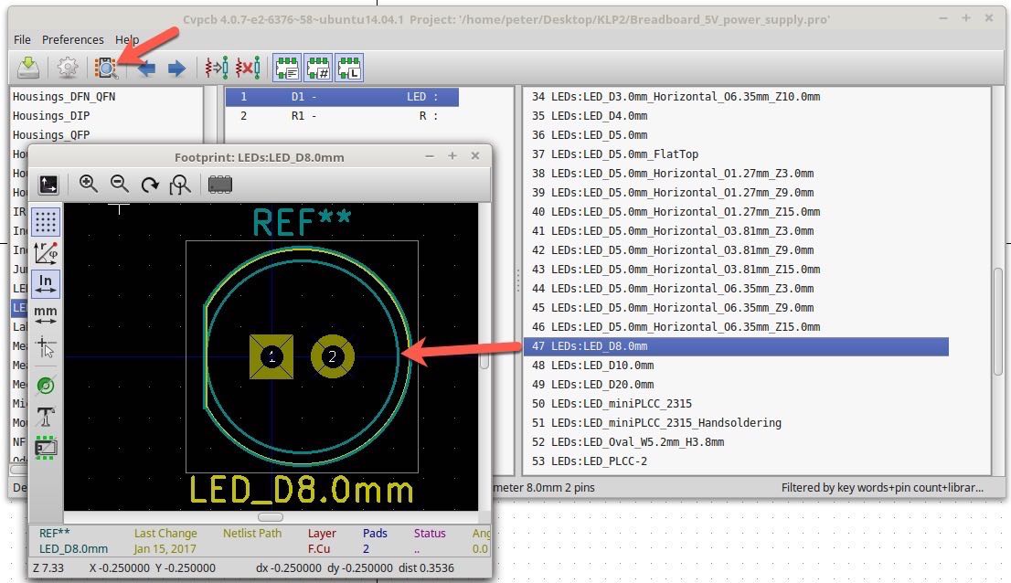
Figure 8.47: A view of the selected footprint.
To complete the association, double click on the footprint item. It will appear in the middle pane, next to the schematic symbol.
Practice this process one more time, and find a footprint for the resistor symbol. In Figure 8.48 you can see what my associations look like.
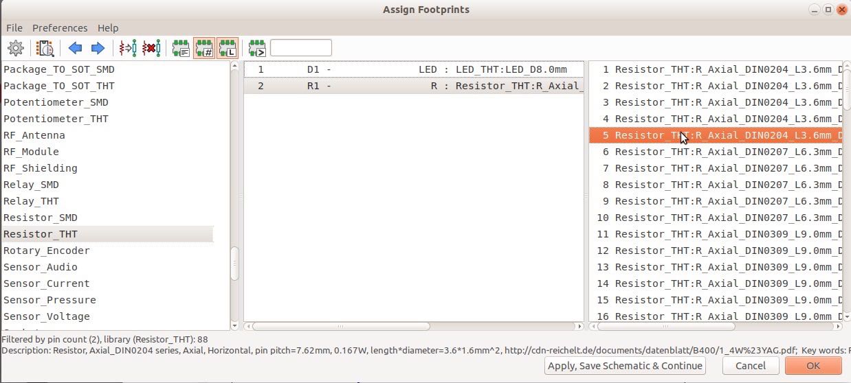
Figure 8.48: The resistor and LED symbols associated with footprints.
Our associations are now complete. Remember to save your work with Cvpcb before you exit this application. You can either click on the disk button in the left of the Cvpcb toolbar or type Ctr-S.
Create the Netlist file
When your schematic is ready, meaning that you have completed drawing it, the ERC has passed, and you have associated symbols to footprints, it is time to continue the work in the layout editor, Pcbnew. Because in KiCad, the schematic editor and the layout editor are two different applications (Eeschema and Pcbnew respectively), there is an intermediate step necessary when you move from Eeschema to Pcbnew.
You must create a file called 'Netlist'.
The Netlist contains information about the symbols, their wiring, and their association with footprints. This information is used by Pcbnew to fetch the footprints from their libraries and place them in the layout design area and to create the ratnets, which are thin lines indicating the electrical connections between the pins that we will need to implemented as as copper tracks.
Let’s go ahead to create the Netlist file for our small circuit. Click on the button labeled '18' in Figure 8.34. It is easy to remember since it contains the acronym 'NET' in its button icon. The Netlist dialog box will appear (Figure 8.49).
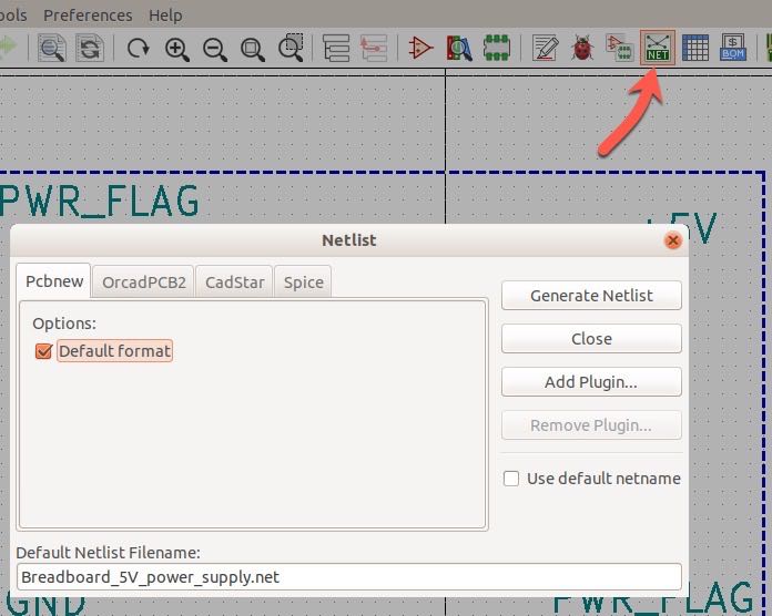
Figure 8.49: The Netlist dialog box.
The Netlist generator can create files that are readable by a variety of layout programs, but since we will be using Pcbnew, we will only work with the Pcbnew tab. Simply click on the Generate button to produce the Netlist file. By default, the Netlist file will be saved in the project directory, which will be easy to find once we get into Pcbnew shortly.
When you click on Generate, a new dialog box will ask you to confirm the save location of the file. Accept the default project directory by clicking on the Save button.
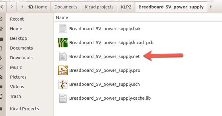
Figure 8.50: The new Netlist file is saved in the project directory.
You can confirm that the new Netlist file is created by looking inside the project directly. It is the file with the '.net' extension in its filename.
Before we continue work on this simple PCB, let have a quick look at the status bar and the menus in Eeschema.
Status bar
The status bar is the area in the bottom of the Eeschema window. You can see an example in Figure 8.51.

Figure 8.51: The status bar in Eeschema.
The status bar contains useful information in five segments. With reference to the labels in Figure 8.51, we have:
1: Status messages such as the total number of nets in a schematic or the next command you are about to select from a menu item.
2: The zoom factor. As you zoom into the sheet to increase the level of detail you can see, the zoom factor also increases.
3: The absolute coordinates of your mouse cursor. The coordinate system in KiCad has its origin in the top left corner of the sheet. The coordinates in segment 3 of the status bar are in relation to the origin (see Figure 8.52).
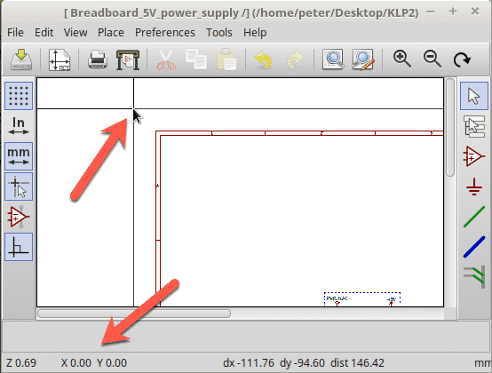
Figure 8.52: The status bar in Eeschema.
4: The relative coordinates, which allow you to measure the distance between two parts of the Sheet. To make a measurement, place the cursor on the location where you would like the measurement to start, and press the spacebar to reset the dx, dy, and list counters. Then, move the cursor to the location where you would like to measure the distance to. The results of this measurement will be in the dx (difference in the x-axis), dy (difference in the y-axis) and dist (absolute distance between the two points) figures.
As an example, let’s measure the distance between the two junction points in our resistor and LED schematic. Place your cursor on the left junction and press the spacebar to reset the counters (Figure 8.53).
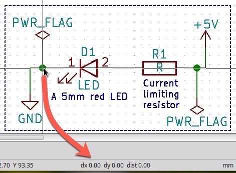
Figure 8.53: Reset the counters by pressing the space bar.
Then, simply move the cursor to the location you want to measure the distance to, let’s say the junction on the right side of the schematic. In the example in Figure 8.54, we learn that the distance is 23.50 mm (dist), as is the difference on the x-axis (dx). The two junctions are on the same location on the y-axis, so the dy value is 0.
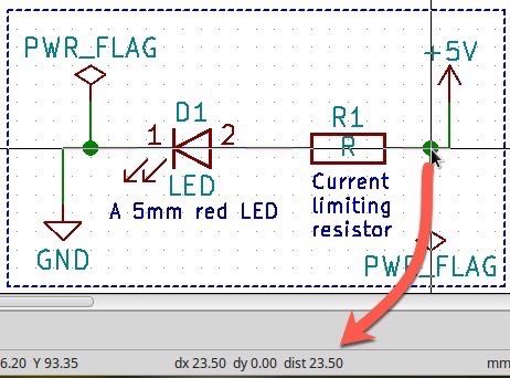
Figure 8.54: Move the mouse cursor to a new location and see the dx, dy and dist counters to update.
5: Show the selected unit of length. I find that the ability to measure distances is extremely important, not so much in Eeschema, but in Pcbnew. In Pcbnew these measurements will help us place a footprint that requires precise physical dimensions. For example, we will use this measurement technique to design a PCB that will fit precisely in our project box, or that will have a screw terminal precisely placed to correspond with a provision for it on our box.
Spend a few minutes to become comfortable measuring distances in Eeschema. It is a skill you will also use in Pcbnew, the component library editor, and the footprint editor.
Menus
To complete our tour of Eeschema, let’s have a quick look at the menus.
The first thing to notice is that these menus contain items that are also available as buttons in the top and right hand toolbars:
- File
- Edit
- View
- Place
- Tools
These two menus contain unique functionality:
- Preferences
- Help
The File menu contains the 'Append Schematic Sheet' item, which is not available as a button. Selecting this item allows you to insert the contents of another schematic sheet into the current sheet. This is useful in cases where you have, for example, a schematics that contains standard circuits, like power supplies and LED arrays. Instead of re-drawing those circuits, you can simply append them into your current design.
Let’s have a look at the Preferences menu. We will not be making any changes there at this time since this is not necessary for the purposes of this small introductory project. But we will be working with the preferences in later projects, especially as you learn to create your own components, or import third-party component libraries (Figure 8.55.
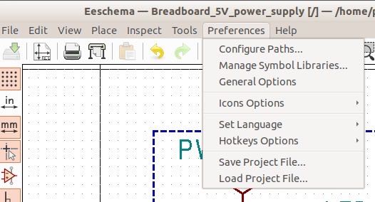
Figure 8.55: The preferences menu item.
From the Preferences menu, click on the Manage Symbol Libraries option. The Symbol Libraries window will appear (Figure 8.56).
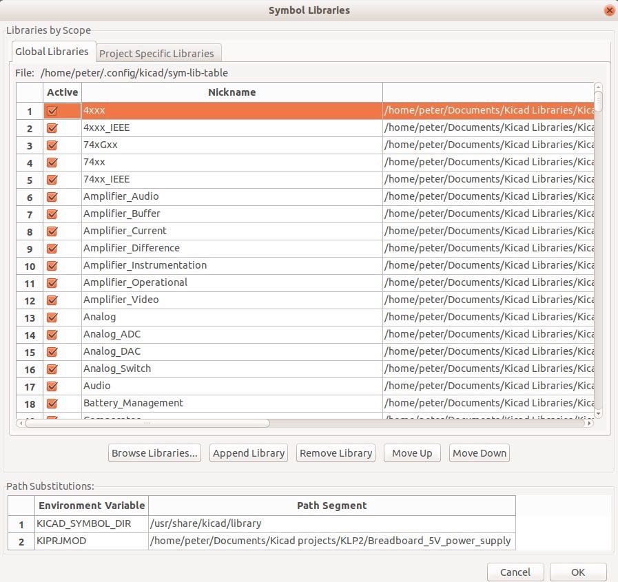
Figure 8.56: The Component Libraries window.
You can use the Symbol Libraries window to manage… symbol libraries. KiCad is endowed with a huge selection of libraries that its users create and share. You can find and install them on your computer using the functions in this window. I will show how to import and use a third-party components library in a more involved project in Section 4 and in the recipe titled 'Adding a schematic symbol library in Eeschema'.
Also look at the General Options window. You are already familiar with the Display, Editing and Controls tabs. Have a look at the Colors tab (Figure 8.57).
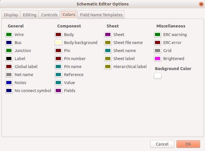
Figure 8.57: The Eeschema Colors Scheme window.
Through the Colors Scheme windows, you can customise the colours that Eeschema uses. You can change the colour of practically any widget and schematic attributes, like wires, junctions, and notes. Simply click on a colour box to bring up a colour chooser and replace the original colour.
In the 'Set Language' Preferences menu item, you can change the KiCad user interface language. KiCad has support for more than 10 languages, but beware that this feature will not work unless your operating system also supports the language you want to choose.
Continuing in the Preferences menu item, you will find the Hotkeys item. You learned about the hotkeys in a previous segment of this book. Here, I will only add that through this menu you can also export and import Hotkeys. This is useful if you use KiCad in multiple computers and you want to have the same Hotkeys configures across all of them.
At the bottom of the Preferences menu, you will find two functions that allow you to save and load your custom preferences to your project file.
KiCad series
Ready to learn KiCad?

Learn the world's favourite open-source PCB design tool with the world's most comprehensive course
KiCad Like a Pro, is available as a video course or as an eBook.
Choose the version that fits best with your style of learning, or get both to get the full benefit of the video demos plus the details of the eBook.
When you complete KiCad Like a Pro, you'll be able to use KiCad to design and manufacture multi-layer PCBs with highly integrated components and a professional-looking finish.
Work through five projects that give many opportunities to learn and practice all of KiCad's important features.
KiCad Like a Pro contains full sections dedicated to PCB and design principles and concepts. These ensure that you will master the fundamentals so that your PCB project are awesome.
If you are someone who is interested in designing PCBs using KiCad, or moving to KiCad from another CAD application, then KiCad Like a Pro, the video course and eBook, is for you.
Jump to another article in this series.
Last Updated 4 years ago.
We publish fresh content each week. Read how-to's on Arduino, ESP32, KiCad, Node-RED, drones and more. Listen to interviews. Learn about new tech with our comprehensive reviews. Get discount offers for our courses and books. Interact with our community. One email per week, no spam; unsubscribe at any time
