10. Design principles and basic concepts
Printed circuit board key terms you should know before you begin
Creating printed circuit boards is an engineering discipline, and as such, it has its own 'language'. In this chapter, you will learn the most commonly used terms so that you can understand the information found in places such as PCB fabrication websites and CAD tool documentation.
Here we go.
FR4
The most common material used to make printed circuit boards is FR4 (or FR-4). This is a glass-reinforced epoxy laminate composite material, or in simpler terms, fiberglass cloth bound using an epoxy resin.
Go over to the Wikipedia article to read more about this material (https://en.wikipedia.org/wiki/FR-4).
The 'FR' part of the name stands for 'Flame Retardant', an obviously desirable quality for a board that will hold together components that can potentially ignite when they fail.
Other useful attributes of the FR4 are:
• Very light and strong
• Does not absorb water
• It is an excellent isolator
• Maintains its quality in dry and humid environments
Apart from the standard FR4 and variants (like FR4 tracking resistant and halogen-free), there are other materials that can be used in rigid or flexible printed circuit boards. Examples include High Tg (HTG) for applications that must operate in high temperates, paper-based materials with PF resins, aluminium, or various kinds of TG rigid and flexible boards.
Trace
Traces (also called 'tracks') are conductive paths. Most often they made of copper. Traces are used to transmit signals and power throughout a circuit.
In Figure 12.1 you can see the traces in the front side of this PCB as thin purple lines that provide the connections between the golden pads where the component terminals will eventually be. You will learn more about pads next.
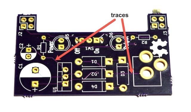
Figure 12.1: An example of traces.
As the designer of a PCB, you have total control over the characteristics of traces. You can control their width, height, and route, including the angles by which a trace changes direction. If you want a trace to be able to accommodate a large current flowing through it with little resistance and temperature rise, you can design it to be wider and thicker. This is useful when a trace is meant to feed power to the components of your board. Traces that are meant to convey low power-current signals (less than 20 mA) can be made narrower, with less copper.
Keeping the width of traces to around 0.3 mm (or even less, depending on your manufacturer’s guidelines) makes it possible to draw traces closer together and reduce the final size of your PCB.
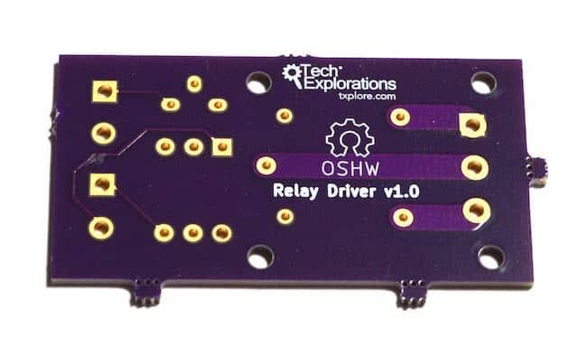
Figure 12.2: An example of wide traces.
In Figure 12.2, you can see an example of traces that are much wider than regular signal traces. These traces connect the terminals of a 240 Volt relay.
The traces in these examples are purple because of the solder mask chemical used to finish the manufacturing process. You will learn about the solder mask further down in this chapter.
Pads and holes
Pads and holes are the most prominent feature of a printed circuit board. Pads come in two varieties and in several shapes. There are TH (through-hole) pads and SMD (surface-mounted device) pads.
In Figure 12.3 you can see an example of a board that contains exclusively TH pads, and in Figure 12.4 you can see a board that contains TH and SMD pads.
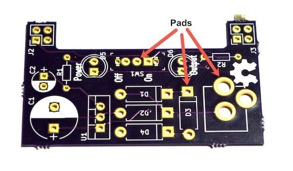
Figure 12.3: Through hole pads.
Through-hole pads, unlike SMD pads, connect the front for the PCB with the back electrically. In the examples, you can see that the gold plating of the pad fills the inside of the hole. If you turn the PCB around, you will see that a matching pad exists in the back.
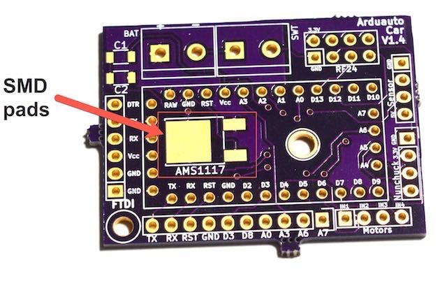
Figure 12.4: An example of SMD pads.
Boards with mostly TH pads are popular among hobbyists because through-hole components are easier to work with, at least in the beginning. SMD components are smaller; hobbyists tend to not use them until they are more comfortable with their soldering skills. I find that with a bit of practice, SMD components are as easy to work with as their TH counterparts.
In the industry, on the other hand, the vast majority of PCBs are designed to contain SMD components. This is because SMD components can be populated on the board automatically using pick and place machines and because their small size results in smaller PCBs.
Apart from the two varieties I described above, pads also come in several shapes. Most often you will see round pads, but rectangular and oval shapes are also possible. Using KiCad, you can create such pads and control their geometry to the extent that your PCB manufacturer allows.
In Figure 12.5 you can see an illustration of a cross-section of a PCB showing the configuration of pads, and two types of holes, Plated-Through Hole (PTH) and Non-Plated Through Hole (NPTH).
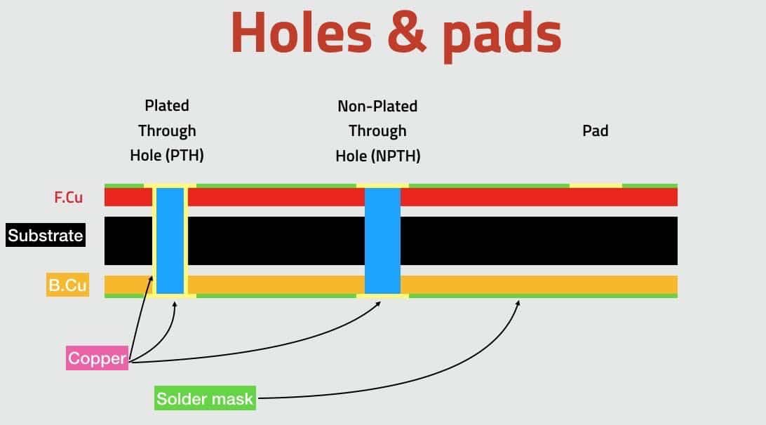
Figure 12.5: Pads and holes.
Plated-Through Holes is the more common variety and the default type of hole in more cases. A drill is used to create the hole, and then copper is used to cover the hole’s sides so that its two ends (at the front and back copper layers) are electrically connected. Vias are constructed in the same way, except that they have a much smaller diameter so it is not possible to accommodate component pins.
On the other hand, in a Non-Plated Through Hole, we use the same drill to create the hole, but there is no copper used to cover the sides of the hole, so there is no electrical connection between its two ends.
Finally, pads without holes are useful for attaching surface-mounted component, as you learned earlier.
Via
When you want to move a signal that travels across a trace from one side of a PCB to another (say, from front to back), you can create a via. A via is a hole with its sides covered with copper or gold (or other conductive material), that allows a trace to continue its route across layers.
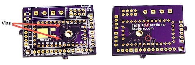
Figure 12.6: Vias allow a trace to continue between layers.
In Figure 12.6, you can see the two sides of the same PCB. On the left, the arrows point to two vias in the front of the PCB, and on the right, the circles indicate the same vias on the back of the PCB. Vias are very similar to through-hole pads, except that they don’t have any exposed copper (they are covered by the solder mask), and they don’t have a pad (so you can’t solder a component).
In simple circuits with only a few components, it is possible to create all of the traces on one layer of the PCB. When a PCB gets busy with more components it quickly becomes impossible to do the routing on a single layer. When multiple layers are needed, vias provide the simplest method of allowing a trace to use the available board real estate.
In the Figure 12.7 you can see the types of interconnections between layers that are possible.

Figure 12.7: Types of interconnections between layers.
For through-hole components, you would design a hole that connects the top and bottom copper layers. This hole is implemented using a drill. It is wide enough to allow for the pin of the component to go through it.
Vias are smaller than holes in terms of their diameter. They are not wide enough for pins to go through them, but they are plated, like holes, and they allow for electrical connection between layers to take place.
A 'through via' is like a hole, but narrower. It connects the top and bottom layers. A buried via is a via that connects any two internal layers. In the four-layer example of Figure 12.7, the buried via connects the In1.Cu and In2.Cu. A 'blind via', also connects two layers, but has one end exposed on to the outside of the board, either top or bottom.
In high-density boards, another option for interconnecting layers is to use a 'micro via' (‘uvia’). A micro via is made using high-powered lasers, instead of a mechanical drill; the use of lasers makes it possible to dramatically reduce the diameter of the via.
Annular ring
The annular ring is a term that describes the area on a pad that surrounds a via. An important related metric is the width of the annular ring, which we define as the minimum distance between the edge of the pad and the edge of the via or pad hole.
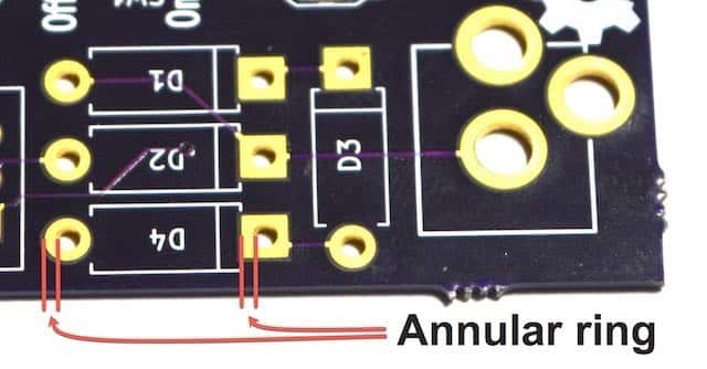
Figure 12.8: Annular rings and width.
In Figure 12.8, the width of two annular rings is indicated with the two red lines. Ideally, the drill hit (the location on the board where the drill lands and creates a hole) is right in the middle of the pad. This is what we usually want. If the drill bit is not aligned correctly, then the hole can be closer to one edge of the pad (a 'tangency'), or it could even miss the pad completely (a 'breakout').
Soldermask
As you know, traces are made of copper. Copper slowly reacts with oxygen in the air, resulting to oxidisation. Oxidised copper produces a pale green outer layer. To prevent this from happening, PCB manufacturers cover the exposed copper with solder mask, a thin layer of polymer that insulates it from oxygen. As an additional benefit, the solder mask also prevents solder bridges from forming between pads.
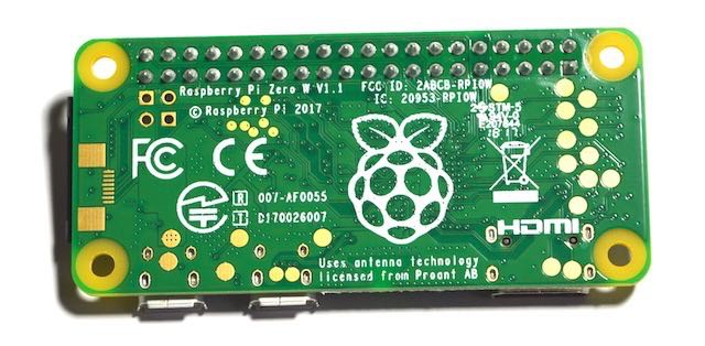
Figure 12.9: The rear of a Raspberry Pi Zero protected with a thin layer of solder mask.
In Figure 12.9, you can see the back of a Raspberry Pi Zero. In this example, the copper is protected by a thin layer of green solder mask. Only the pads and the mounting holes are not covered by the solder mask.
Solder mask polymers are available in different colours, with green being the most common and cheaper. You can create fancy looking PCBs with black, blue, red, purple and many other colours.
Silkscreen
Printed circuit boards are not complete without text and artwork that convey useful information and add a touch of elegance. In Figure 12.9 you can see an example of such text and artwork on the back of a Raspberry Pi Zero. You can see the Raspberry Pi logo, logos of various certifications, and various text items that inform us about the model etc. All this consists of the silkscreen.
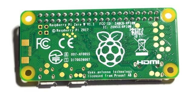
Figure 12.9: The white text and graphics on this Raspberry Pi Zero consist of the silkscreen.
The name 'silkscreen' is rather misleading. Of course, no actual silk is used to produce the white elements on the PCB. The method used to print the silkscreen in large numbers is a relative of the traditional screen printing process that you can use to print a graphic on a T-shirt. The silkscreen text and graphics are printed on the boards while they are still in their panels.
White is the most common colour for the silkscreen, but black and yellow are also available.
In the projects that you will work through later in this book, you will spend a considerable amount of time creating the informational and decorative text and graphics in the silkscreen layer of the PCB.
Drill bit and drill hit
Drill bits are used to create holes and vias, but also cutouts. Drill bits are typically made of solid coated tungsten carbide material and come in many sizes, like 0.3 mm, 0.6 mm and 1.2 mm. The look like the one in Figure 12.10. These drills are attached to computer controlled drilling machines and are guided by a file that contains information about the coordinates and the drill size for each hole on the PCB.
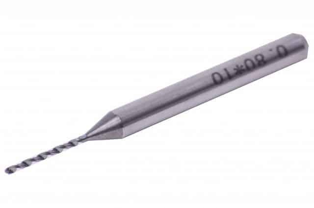
Figure 12.10: An example drill bit.
It is interesting to note that for very small holes, usually vias, drill bits are replaced with lasers. These vias are often called 'micro-vias'. With laser drilling, it is also possible to create vias that connect in-between layers of the PCB.
The term 'drill hit' describes the location on the PCB where the drill bit comes in contact with the PCB and creates a hole.
Surface mounted devices
If your objective is to create a PCB that is easy to manufacture in very large numbers, with a minimum size, then you should design it to contain surface mounted components instead of through-hole components.
In Figure 12.11 you can see an example of what is possible to do with SMD on a board. A full computer, on a tiny board, for a few dollars.
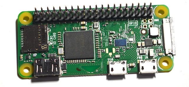
Figure 12.11: The Raspberry Pi Zero contains almost exclusively SMD components.
On this board are a highly integrated microprocessor, memory, communications, and connectors. Even the connectors are SMD. In fact, the only component that is through-hole is the header.
Creating something like this using through-hole components, if at all possible, would result in a board that was many times the size of the Raspberry Pi Zero, and would cost many times more because most of the assembly would have to be done by hand.
While hobbyists prefer to work with TH components because they are easier to solder and repair, learning to work with SMD, at least the larger ones, is certainly possible.
In this book, you will learn how to create an SMD version of a PCB, in addition to the TH version.
Gold Fingers
Appropriately called 'Gold finders' are gold-plated connectors placed on the edge of a PCB. Gold fingers are useful for interconnecting one board to another. You can see an example in Figure 12.12. This is the micro:bit educational single board computer.
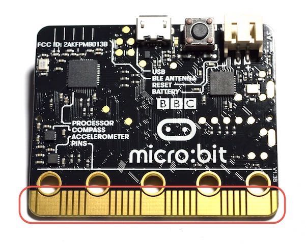
Figure 12.12: Gold fingers on a Micro:bit.
The micro:bit uses its gold fingers to connect to other devices, like motor controllers and sensors, via a slot. Gold fingers, when manufacture properly and with sufficient thickness, makes it possible to attach and detach the PCB to a slot at least 1,000 times before they start to wear out.
Panel
To manufacture PCBs economically, manufacturers use machines that can work on large panels. Each panel can be designed to contain many copies of the same PCB. It is also possible to use clever algorithms that place different PCBs on the same panel so that the capacity of the panel is fully utilised, and that the individual cost of each PCB is reduced. This is how it is possible to have a single 'hobby' PCB manufactured for a few dollars. This panelisation process is key to this reduction in costs.
In the example of Figure 12.13, a single panel contains four individual PCBs. The four PCBs are populated while they are still part of the panel using an automated pick and place machine. A pick and place machine is a robot that uses an arm to pick each component from a container and places it precisely on the pads. Once the components are on the board, the panel moves into the next step of the process in which they are 'baked' and secured in place.
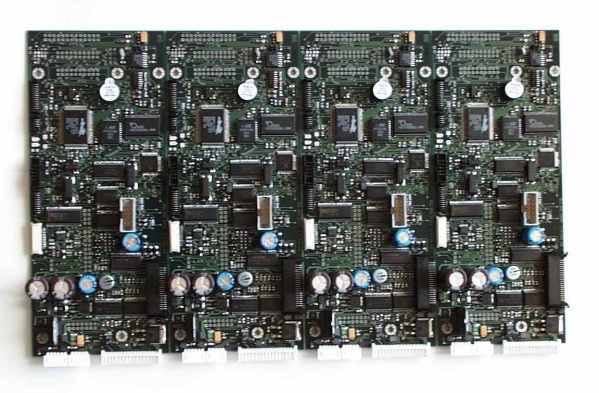
Figure 12.13: A panel with three individual PCBs.
To remove the PCBs from the panel, manufacturers utilise defined breakaway routes and points on the board to snap them off. In Figure 12.14 you can see the breakpoints along the edges of this PCB.
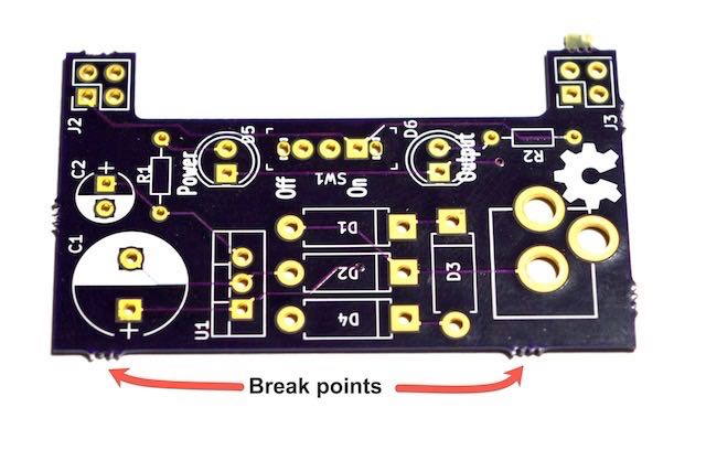
Figure 12.14: This PCB used to be part of a panel.
Using a drill, the manufacturer removed the substrate material in between the breakpoints so that with a small amount of force, individual PCBs can break free from the panel without damage.
Solder paste and paste stencil
Solder paste (or solder cream) is a soft and sticky material (at room temperature) that is applied on pads in preparation to attaching a component. Think of solder paste as normal solder. While with normal solder you will need a soldering iron to heat it, melt it, and apply it on a component pin that is already in place, with solder paste you will first use a syringe (or one of the other application methods) to cover the pad, then place the component on the pad, and provide heat in the form of an oven to heat the paste and bond it with the pad and the component’s plated area.
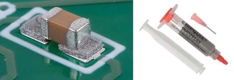
Figure 12.15: Solder paste in a syringe dispenser, and an SMD component.
In Figure 12.15 you can see an example of a solder paste in a syringe dispenser, that you can purchase from retailers like RS Components. Using the syringe equipped with a thin nozzle, you can manually deposit a small amount of solder paste on the pads. Using tweezers, you can place the component you want to attach on the solder paste. Because solder paste is sticky (before it’s baked), the component will attach to it. Once you have all the components you want on the board, you can place it in an oven to bake it. After the baking process is complete, the solder paste will be solid, like normal solder. The SMD components will be mechanically secure and electrically connected to the pads.
Solder paste also comes in a tub, which is more appropriate for application to a board using a stencil (Figure 12.16). Stencils are useful in large-scale productions.
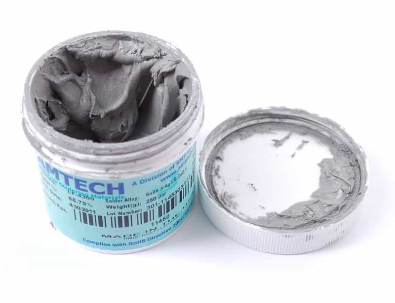
Figure 12.16: Solder paste is a tub container.
A stencil, typically made of stainless steel, is cut so that it has openings of the exact size and the exact location of the pads of the board. The technician will place the stencil over the board, and then apply the paste on the openings. When the stencil is removed, the paste remains on the pads only.
Then, either manually or using an automated pick and place machine, the components are placed on the pads and stick on them because of the paste. The last step is to bake the board in a reflow in order to solidify the paste.
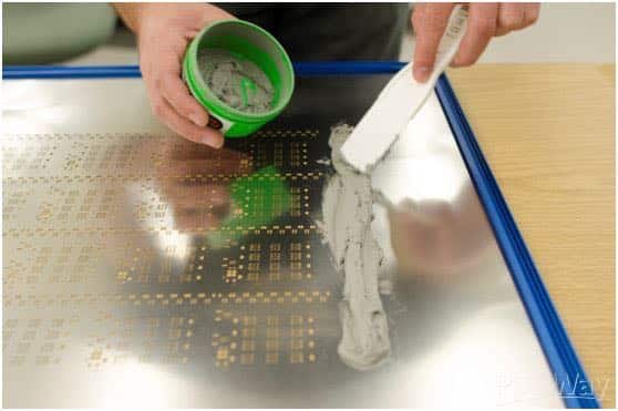
Figure 12.17: A stencil, with solder paste being applied using a squeegee (photo courtesy of Pcbnew.com).
A reflow oven is an industrial-sized machine that is used to complete the process of attaching SMD components on a PCB. You can also purchase or make a reflow oven for use at home. People have even made reflow ovens for their projects using discarded toasters. In either case, a reflow oven is designed to operate under a specific program that controls the amount of heat a board receives over time. This is important because the heat must be appropriate for the purpose of converting the solder paste into good-quality electrical connections, without causing damage to the board or the components on it.
Pick-and-place
Pick and place machines are robots that assemble the various components on the surface of a circuit board. When you contract a manufacturer to not only make your boards but also to populate them, they will be using a pick and place machine. You can see an example of a pick and place machine in Figure 12.18.
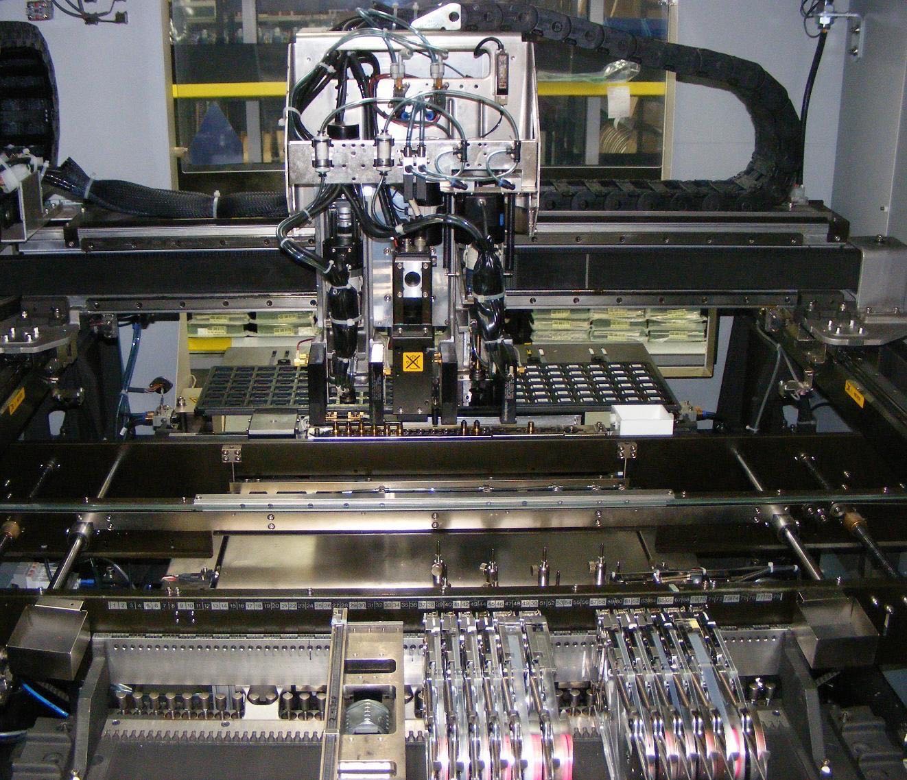
Figure 12.18: A large pick and place machine (By Peripitus [GFDL (http://www.gnu.org/copyleft/fdl.html) or CC BY-SA 3.0 (https://creativecommons.org/licenses/by-sa/3.0)], from Wikimedia Commons).
A typical pick and place machine, like the one in Figure 12.18, includes:
- a repository of the various components that are to be placed on the board,
- a conveyor belt that brings in the boards,
- an inspection system composed of cameras that can optically recognize the board, components and other guidance markings on the board,
- a robotic arm that can pick a component from the repository and place it on the board (these arms are usually fitted with suction cups so they can pick and manipulate components).
Modern high-end machines are very versatile, optimized for short runs of complicated boards, and artificial intelligence designed to assembled and test boards ensuring high levels of reliability.
KiCad series
Ready to learn KiCad?

Learn the world's favourite open-source PCB design tool with the world's most comprehensive course
KiCad Like a Pro, 3rd edition is available as a video course or as an eBook.
Choose the version that fits best with your style of learning, or get both to get the full benefit of the video demos plus the details of the eBook.
When you complete KiCad Like a Pro 3e, you'll be able to use KiCad to design and manufacture multi-layer PCBs with highly integrated components and a professional-looking finish.
Work through five projects that give many opportunities to learn and practice all of KiCad's important features.
KiCad Like a Pro 3e contains full sections dedicated to PCB and design principles and concepts. These ensure that you will master the fundamentals so that your PCB project are awesome.
If you are someone who is interested in designing PCBs using KiCad, or moving to KiCad from another CAD application, then KiCad Like a Pro, the video course and eBook, is for you.
We publish fresh content each week. Read how-to's on Arduino, ESP32, KiCad, Node-RED, drones and more. Listen to interviews. Learn about new tech with our comprehensive reviews. Get discount offers for our courses and books. Interact with our community. One email per week, no spam; unsubscribe at any time
