12. Design principles and basic concepts
PCB layout workflow in Kicad with pcbnew
In a previous article in this series, you saw a high-level view of the process of creating a PCB in KiCad. The process starts with the design of the schematic diagram that describes your circuit using Eeschema, and concludes with the layout of the physical components of the PCB using Pcbnew. KiCad contains other tools that assist us in this process, like the footprint and component editors and Cvpcb which allows us to associate components to footprints.
In this article, we'll focus on the PCB layout step of the process. In KiCad, this is the step that involves Pcbnew. This is because I perceive the layout step as the one that uniquely shapes the final 'real world' product. What it will look like, how well it will function, how 'manufacturable' will it be, how durable it will be; all this depends on the layout step.
The process I describe in here is applicable to any PCB layout tool, although I will be using KiCad terminology where necessary to make it easier for you to associate the process with the functionalities inside Pcbnew.
You can see the process in Figure 14.1. For simplicity, I have rendered it to look linear. In reality, the process is iterative. It is often necessary to move, for example, from step 3 back to step 1 in order to adjust the grid so that parts fit better in the available space. Having said that, this diagram should help you understand the steps through which every PCB design has to go through. In this chapter, I will describe each of those steps. Once you apply this process to the projects in Part 4 of this book, it will become 'natural'.
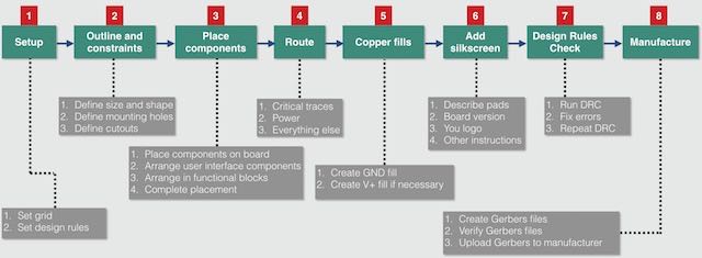
Figure 14.1: A serialized view of the PCB layout process.
Step 1. Setup
In the setup step, you configure the Pcbnew drawing grid size, the layers and set the design rules for the layout. The grid size and number of layers depends on the dimensions and complexity of your PCB. The design rules are governed mostly by the constraints set by your PCB manufacturer, but also by the requirements of your project. Let’s start with the grid first.
The grid provides assistance with the placement of footprints, drawing of traces, and the drawing of the cutout (boundary) of your PCB. Pcbnew provides multiple grid sizes, but you can also define your own custom size.
When you start a new project, select the grid that is most appropriate for the design of the board’s outline and the placement of the footprints. Typically, we will choose a larger grid size for the outline, and a smaller one for the footprints. We may go for a third, smaller grid size to help with the drawing of the traces as this often needs to negotiate tiny details on the PCB, like going around pads and vias.
Larger grids produce more coarse drawings.
Let’s say that you want to produce a rectangular PCB that measures 50 mm by 30 mm. On it, you want to place a few resistors, LEDs and headers. A reasonable grid choice for the outline and the larger features is 1.27 mm, and half that (0.635 mm) for the components. When you start work on the traces, you can consider going one level down from 0.635 mm, to 0.508 mm or even 0.2540 mm if there are too many pads to connect.
The larger grid will allow you to draw the cutout of the board in precise 1.27 mm segments. With this grid, you will be able to draw the long side (50 mm) with 39 x 1.27 mm segments, for a total length of 49.53 mm, or with 40 x 1.27 mm segments for a total length of 50.8 mm. If you need to go for an exact 50 mm side, then you can define a custom grid side, say 0.5 mm, using the Grid Setting dialog box (Figure 14.3), and select it from the Grid drop-down menu (Figure 14.2).
Once you are finished drawing the cutout, you can switch to the smaller Grid side and continue by placing the footprints inside the board.
KiCad makes it easy to switch between two grid sizes by using the grid fast switching shortcuts. The default shortcuts are Alt-1 and Alt-2, although I have changed this to something else to avoid conflict with the Ubuntu operating system’s Alt-[X] shortcut that allows fast switching between applications (where 'X' is the number of the application on the taskbar).
To define which grid size you want to work with, use the Grid drop down menu (Figure 14.2).

Figure 14.2: Select your working grid from the top menu.
After the grid size, you need to define and confirm the number of layers you want to use and the design rules. In regards to the number of layers, the vast majority of hobbyist projects seem to be best implemented with two layers. The best online manufacturers have optimised their processes to work with two layers, both from a cost and also quality perspective. Even if you create a single-layer PCB design, these manufacturers will use a two-layer process on it, and therefore the cost will be the same. If you are creating a more complicated PCB, you can setup Pcbnew for more than two layers. You can select the number of layers for your PCB from the Layer Setup dialog box, that you can reach from the Setup menu (Figure 14.4).
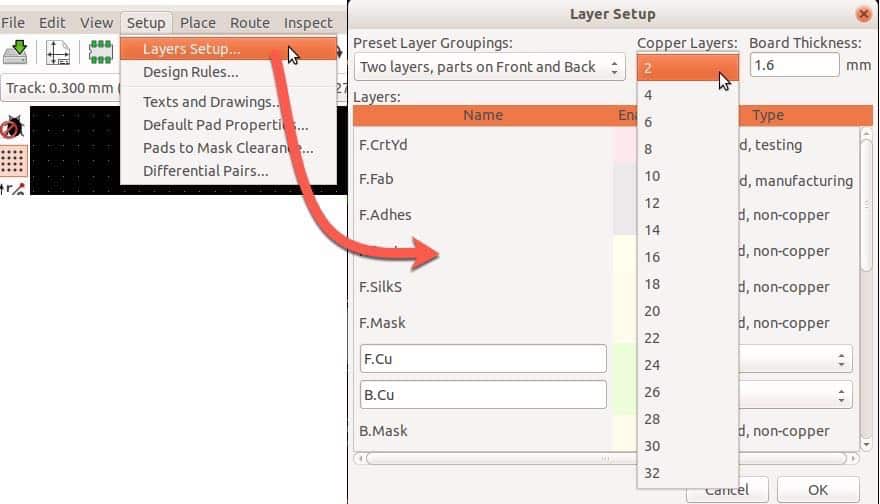
Figure 14.4: KiCad can produce PCBs with up to 32 layers.
The last item in the Setup todo list is to define and confirm the Design Rules. The design rules that you want your PCB to comply with are dictated by your project’s technical requirements but also by your preferred manufacturer’s capabilities and guidelines. To set up your project’s design rules, open the Design Rules Editor from the Setup menu. In Figure 14.5 you can see the editor with the default values for one of the projects in this book.
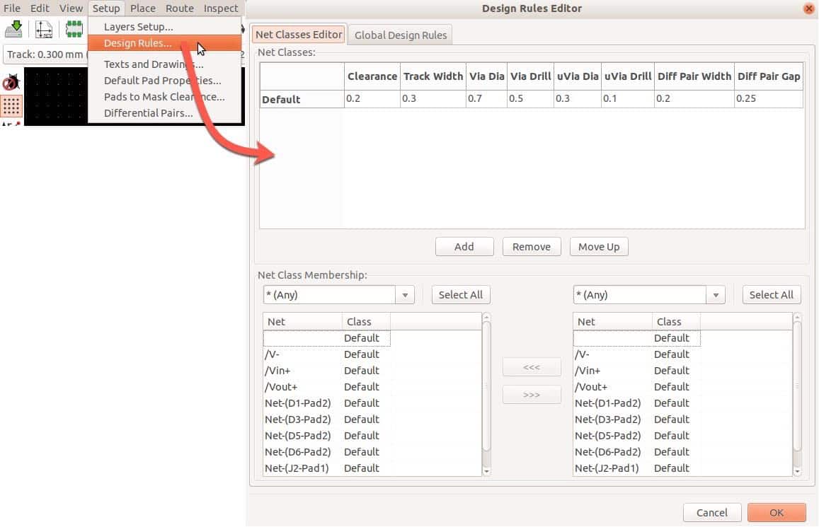
Figure 14.5: The Design Rules Editor with its default settings.
When starting a new project, it is a good habit to confirm that at the very least, the design rules are compatible with the guidelines set by your preferred manufacturer. The best online manufacturers publish these guidelines on their website. For example, OSHPark has a web page[9] with design rule information specifically for KiCad, where we learn that the minimum track (trace) width is 0.006' and the minimum via diameter is 0.027'. PCBWay also publishes this information in a page on their website,[10] where we learn that their minimum track (trace) width is 0.1 mm and minimum drill size is 0.2 mm. Beware of the units that manufacturers report these numbers as they may be in imperial units (inches), metric (mm), or in mil.
You should ensure that the values in the Design Rules editor, both in the Net Classes Editor tab and in the Global Design Rules tab, are equal or larger to those that your manufacturer specifies as a minimum. If you want to be able to manufacture your boards with multiple manufacturers, then you must ensure that your design rules comply with the largest minimum of their requirements.
The default values in the Design Rules Editor are larger than the minimum values of both OSHPark and PCBWay, so I usually don’t make any changes to them. I do, however, add at least one new row in the Net Class Editor tab to define larger track widths and vias for power tracks as these convert more current compared to the default (signal) tracks. You will learn how to do this in the projects. There is also a recipe in Part 5 where you can learn how to do this quickly.
Step 2. Outline and mechanical constraints
The next step in the process is the definition of the board outline. This outline defines the shape of your board. It is good practice to define the shape of your board before you add any components to it so that you can ensure that it will fit properly within the confines of a project box or other mechanical constraints.
Apart from defining the shape and the dimensions of your PCB, this is the step where you must also define fixed features such as mounting holes and cutouts. Again, these items must match your project box or other external mechanical constraints. If you don’t deal with these issues now, it is likely that you will have to relocate components and traces later, a much more tedious exercise. In Figure 14.6 you can see the board outline from one of the projects in this book. I have unchecked all layers except for Edge.Cuts to make is easier to see the yellow line of the board outline.
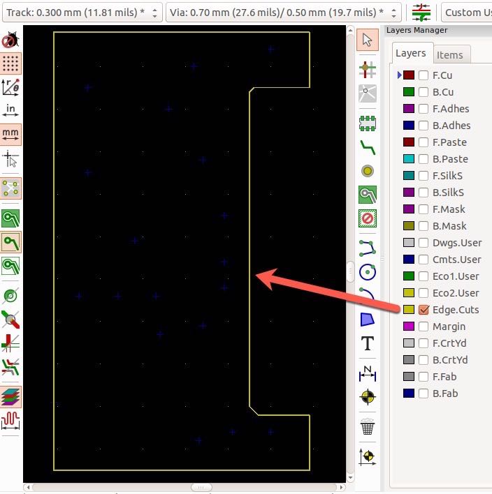
Figure 14.6: Define the board outline in the Edge.Cuts layer.
To define the outline and the cut outs of a board, select the Edge.Cuts layer from the layers manager and use the graphics tools to draw it. As mentioned in the Setup section, I prefer to use a large grid size while I am drawing the outline.
The easiest shape you can draw for your PCB is rectangular. However, using Pcbnew’s Arc and Circle graphics tools you can create elaborate non-rectangular shapes that will make your PCB stand out. In the projects in this book, we’ll use these tools to create rounded corners and other interesting features. If you can’t wait to learn how to do this, you can jump to the 'Irregular shaped PCB’s' recipe in Part 5 of this book.
To create mounting holes and cutouts, you can choose one of a couple of methods. You can create them in the Edge.Cuts layer, or using pads during the component placement step. If your preferred manufacturer supports the first method, then I suggest you go with that as it is faster and helps to keep your design clean because you are not mixing the electrical and mechanical aspects. See an example in Figure 14.7.
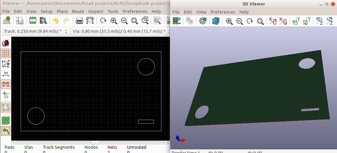
Figure 14.7: You can create openings within the outline of the PCB in Edge.Cuts if your manufacturer supports this method.
In this example, I have created a simple rectangular PCB. Within it, I used the circle graphics tool to create two round openings (screw holes), and the polygon tool to create a small rectangular opening. You can learn more about how to create openings by jumping to the Creating mounting holes and openings recipe.
Step 3. Placement of components
After we have defined the mechanical characteristics of our PCB we can proceed by placing the components (called 'footprints' in Pcbnew) on it. Like everything in engineering (and in life, in general) a good amount of thinking and planning here will pay off dividends later in the form of fewer errors and need to move things around in order to fix those errors.
When you import the project footprints to PCBnew by reading the netlist file, all of the footprints are arranged in a matrix adjacent to each other.
Continue by placing in position the footprints that make up the user interface of your PCB. These are things like connectors, indicator LEDs and buttons. You can see an example of this placement process in Figure 14.8.
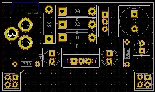
Figure 14.8: An example outcome of the component/footprint placement step.
In this example, I started the placement process by positioning the user interface components along the edges of the board. You should think carefully where to place those components. For example, at the top left of the board, you can see the barrel connector. A cable will plug into this component. Therefore there is a requirement here to ensure that there is sufficient space around the board for the cable. I could have placed the connector facing in the opposite direction, but then the cable would interfere with my work in the breadboard. In Figure 14.9, you can see how the barrel connector, in the top left corner of the PCB, makes it easy to connect the power supply without obstructing the use of the breadboard.
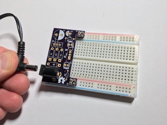
Figure 14.9: Consider the user interface requirements of your PCB carefully.
Other parts of the user interface are the mini slide switch, the two indicator LEDs, and the headers. The headers consist the mean by which the power supply PCB plugs into the breadboard, so their positions are severely restricted by the geometry of the breadboard. I actually placed these components first and locked them in place.
I have more freedom to decide the position of the slide switch. My final decision was guided by the principle of placing UI components along the edges of the PCB for easier access, and ergonomics. I felt it would be easier to reach the switch if it was away from bulky components (like the large capacitor) and closer to the breadboard. I placed the two LEDs around the switch after I had locked the switch in place. Apart from better ergonomics, the LEDs are electrically connected to the switch so it makes sense to place them close as this results in shorter traces.
Once I had finalised the positioning of the UI components, I continue with everything else. I followed these principles:
1. Components that are functionally related should stay close to each other.
2. Shorter traces are better.
3. Consider how placement will affect assembly.
4. Consider component manufacturer specifications.
The four diodes belong to the same functional block (the bridge rectifier), so I placed them as closely as possible. The same applies to the two capacitors and the voltage regulator (the regulator stage). Finally, I placed the current limiting resistors close to their LED for the same reason.
In this example, there is no particular manufacturer specification that I had to take into consideration, other than providing sufficient space for each component. In other cases, however, you may have to deal with components that need, for example, specific provisions for removing excess heat. This can be done by providing additional space for a heat sink, or provide thermal vias for the same purpose. Thermal vias are vias that are not connected to a trace. They are useful for moving heat away from a component, such as an integrated circuit, through a die-attached paddle in between the via and the component. If the manufacturer specifies this as a requirement, you should implement the heat vias or other provisions in this step.
With the components placed on the board, the next step of the process is the routing of the traces.
Step 4. Routing
With the component placement step complete, you can move on to the next step, routing the traces. This step involves the drawing of the copper connections between the pads. To implement the traces between the pads, you can follow this process:
1. Start with any critical traces. This could include signal traces that have specific shape and length requirements, like an onboard antenna.
2. Continue with power traces.
3. Finish with the rest of the traces.
Let’s have a look with an example of what a critical trace might look like. In Figure 14.10 you can see the front and back view of the Microbit board. The Microbit includes a trace Bluetooth antenna. You can see its trace in the top left corner of the front of the board (left image). Because the antenna has strict geometrical specifications for it to operate properly (and legally), it is the first trace that is placed on the board. In the right image of Figure 14.10, you can see the back of the board. In the top right corner of the back of the board you can see that the area of the antenna has nothing on it. No components, and no traces. This is a 'keep out' zone, an area that we can define on a board to make sure that the autorouter or we cannot place anything there. Doing so would affect the way that the antenna works.
To learn how to create a keep out area you can refer to the relevant recipe.
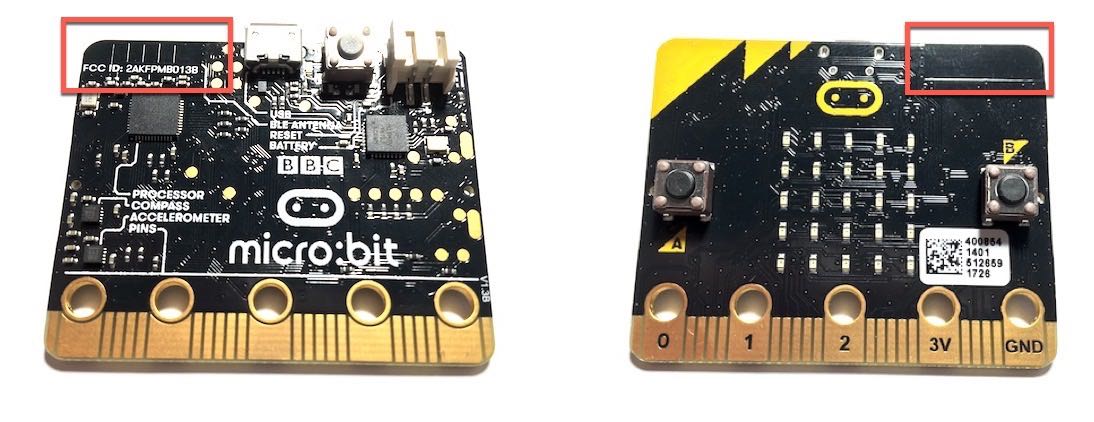
Figure 14.10: The integrated antenna in this Micro:bit is a critical trace.
Once you have taken care of critical traces, if any, continue with power traces. Power traces travel throughout your circuit to feed it with power, and as such, they convey a higher current then signal traces. For this reason, it is appropriate to design power traces (GND, 5V, 3.3V etc) so that they are wider than normal signal traces. For low voltage and low power consumption boards, power traces should be around 0.30 mm to 0.40 mm in width. The trace width depends on a few variables and you can learn more about it in the Trace Width Calculator recipe. You can learn about using net design rules to automatically define the width of a trace in the custom net design rules recipe, or how to adjust the trace width manually in the custom design rules recipe.
After you have completed the routing of the power traces, you can continue with the rest of the traces. For larger boards, you can setup an autorouter that can save you some time. For smaller boards, you can finish routing manually. You can learn about the autorouter in the relevant recipe.
Before continuing to the next step, run the Design Rules Check process to make sure no defects have been introduced.
Step 5. Copper fills
This step is not necessary and often designers decide to skip it. Copper fill is an area on the board that is fully covered with copper.
Typically, copper fills (also known as 'copper pours') are used to create a ground plane, which is a contiguous mass of copper connected to electrical ground. Similarly to a ground plane, you can create copper planes connected to a voltage level. If your PCB draws power from a battery, then the ground plane is connected to the negative electrode of the battery, and a voltage plane is connected to the positive electrode of the battery.
When a copper fill is created, pads can be connected to the fill using a small number of very short traces called ‘thermal reliefs’ (or 'thermals' for short). You can see an example of this in Figure 14.11.
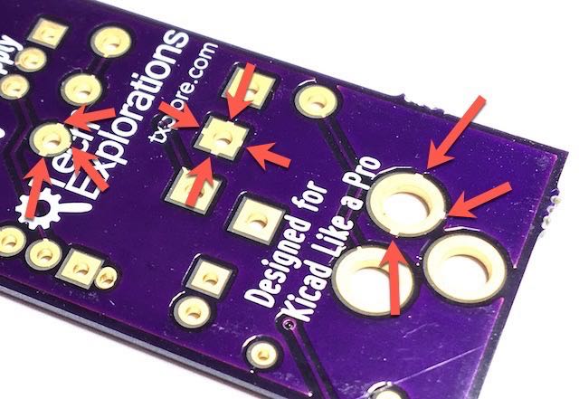
Figure 14.11: Arrows show where GND pads use thermals to connect to the GND plane.
In this example (the breadboard power supply board project from this book), you can see how multiple GND pads are connected to the ground plane in the back of the PCB using up to four short traces. The purpose of the thermals is to help with the soldering of the components on the pad. If the pads were connected to the plane with a full complement of copper, the heat of the soldering iron would dissipate into the copper fill too fast, and the pad would not be able to reach a temperature suitable for the solder to melt. To reduce the heat dissipation speed, the thermals are used to ensure electrical conductivity while managing the heat from the soldering iron.
The distance between the copper fill and traces that belong to a different net is termed 'backoff' or 'standoff'.
Copper fills may be made to be solid, or using a pattern like a 'cherry pie lattice'. Modern copper pours are almost always solid. In the past, cherry pie lattice or hatched patterns were used to prevent wrapping, but this does not seem to be a problem anymore. I have never experienced wrapping in my boards using a solid copper fill.
The benefits of using ground copper planes are:
- They offer a degree of protection against electromagnetic interference
- They help to dissipate heat produces by the board components
- They enforce the discipline of placing signal traces on the top layer and connecting all ground pads to the bottom ground copper plane using vias.
To learn how to create a copper fill, please refer to the relevant recipe in Part 5. As you will see, the process is very similar to creating a keep-out zone.
A copper fill is created once all routing is completed. In a typical 2-layer board, a ground plane is created in the bottom of the PCB, and often a V+ (say, 5 V) copper fill is created on the top layer. If your board is using multiple layers and multiple voltages (like 3.3 V or 5 V), then another option is to use the bottom layer for the ground plane, one of the middle layers for the positive voltages, and the top layer for the signals.
Before continuing to the next step, run the Design Rules Check process to make sure no defects have been introduced.
Step 6. Silk screen
Step six of the PCB design process is the silkscreen artwork. Silkscreen artwork can be placed on the top and bottom layers. KiCad offers two special layers dedicated to the silkscreen: 'F.SilkS' and 'B.SilkS'. In general, the silkscreen artwork involves the following elements:
- Descriptions of pads (i.e. what is the role of each pad). This is done using text characters.
- A name and version number of the board, also in text characters.
- Your logo, and other graphics you may want to include.
- Other instructions that may assist the end user, like names, models and values of components, input and output voltage levels, and email address or a website where the user can look for more information.
Let’s have a look at an example of these elements in the board you can see in Figure 14.12.
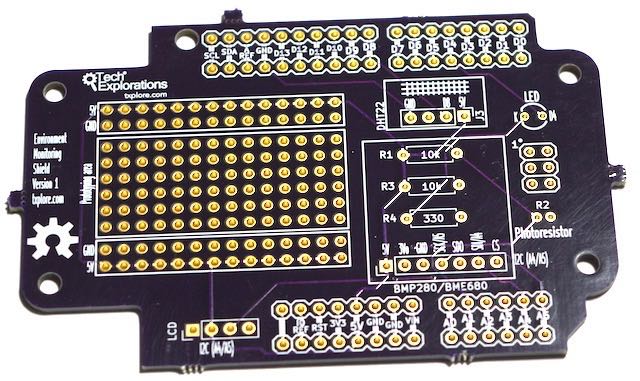
Figure 14.12: The silkscreen information on this board improve its usability.
The board in Figure 14.12 is one I designed for one of my Arduino courses. I designed it as an Arduino shield. It contains a prototyping board, and has provision for a DHT22 sensor, a BMP280 sensor, a photoresistor, and LED, and exposes the I2C interface so I can connect an LCD screen. When fully assembled and stacked on an Arduino Uno and an Ethernet Shield, it looks like the example in Figure 14.13.
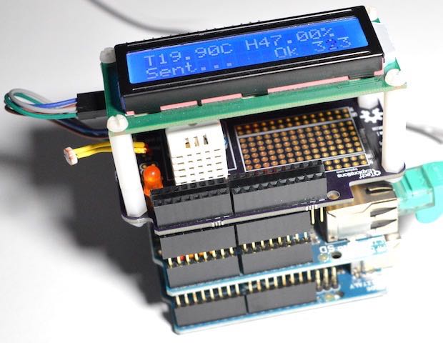
Figure 14.13: The Environment Shield in operation.
In Figure 14.12 you can see the contents of the top layer silkscreen in white ink. The Tech Explorations logo, with a URL, and the 'open-source hardware' logo appear on the left of the board. The name of the board and its version appear at the left edge of the board. Each pad has text that describes its purpose; the BMP280 and DHT22 pads are marked. There is also information on the values of the resistors, and the cathode of the LED is marked. All this information will help the end user to assemble the board without the need for a reference document.
The prototyping area is also marked. The row of pins that convey the GND and 5V levels are clearly marked. The bottom layer can also have a silkscreen where you can provide additional information. Because the bottom layer typically does not have components, there is more available real estate to use for this purpose.
Spending some time to design a beautiful and informative silkscreen adds significant value to your board, so it is worth the effort. Because there is no automated test, like the DRC, for ensuring that the information in the silkscreen is correct, you should take care to manually check and double check that there are no errors. Much of the silkscreen text and graphics belong to the footprints themselves. If the footprints come from a quality source, like the KiCad repository, the risk for errors is low, but it is still prudent to check your self. For example, in Figure 14.12, the LED footprint came with its own silkscreen graphics. The circle around the pads is part of the footprint. But to make the assembly process easier, I added the 'K' designator to indicate the cathode pad so that the end user would know how to connect the LED. The shield pad markings ('A0', 'A1', 'SCL', 'SDA', etc.') are all part of the Arduino shield footprints that I imported into the project. While I modified the footprint to add space for the prototyping area and the LCD screen, I left the silkscreen text in place.
To learn how to insert graphics, such as a logo, to the silkscreen, please refer to the relevant recipe. There is also a recipe that shows how to insert silkscreen text and simple graphics to the top or bottom layer.
Step 7. Design Rules Check
The seventh step of the PCB design process is the Design Rules Check (DRC). While it is a good habit to run the DRC frequently, and at least every time you complete major trace routing or adding a copper fill, you should always run it when you are satisfied that the design work is complete and before you send the board to your manufacturer.
To start the DRC, click on the DRC button which is located in the top toolbar. In the DRC window (Figure 14.14), click 'Start DRC' to run the basic check. If it all goes well, the Problems and Unconnected tabs will remain empty.
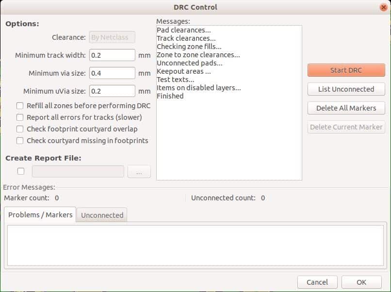
Figure 14.14: The DRC window; this checked returned no errors.
The DRC window allows several check options. You can get it to automatically refill zones before performing the DRC, to report all errors for tracks, and do a couple of courtyard checks, like courtyard overlap and footprints with missing overlaps. A footprint courtyard is defined by the KiCad documentation[11] as the smallest area that provides a minimum electrical and mechanical clearance around the component. Footprint courtyard layers are F.CtrYd and B.CtrYd.
When I did the DRC again in my project board, with all options selected, as you can see in Figure 14.15, the DRC returned one problem that indicates that one of the board’s footprints has no courtyard defined.
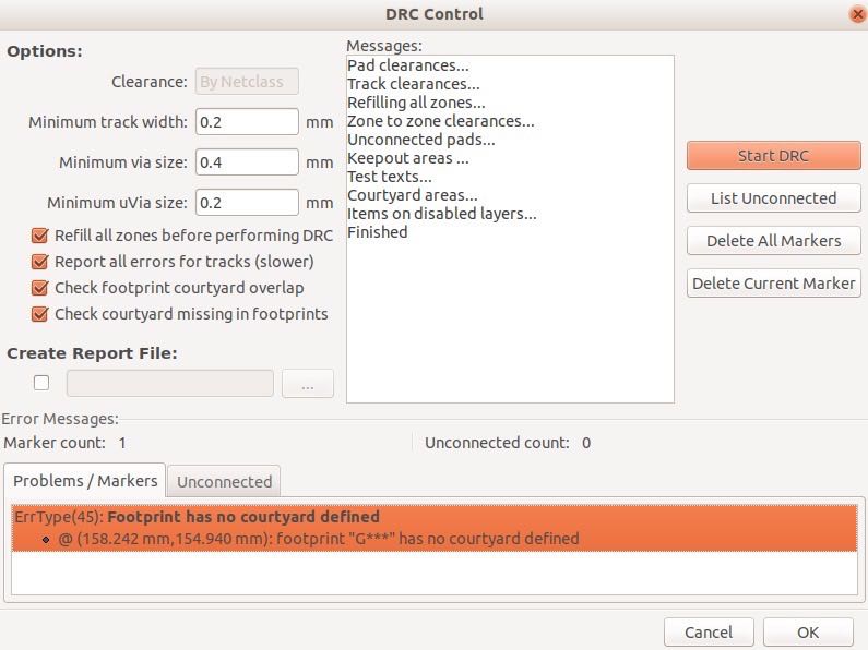
Figure 14.15: This DRC returned one problem.
To investigate the problem, I turned off the filled zones so I can see the board with more clarity. The DRC arrow in Figure 14.16 indicates the problem area.
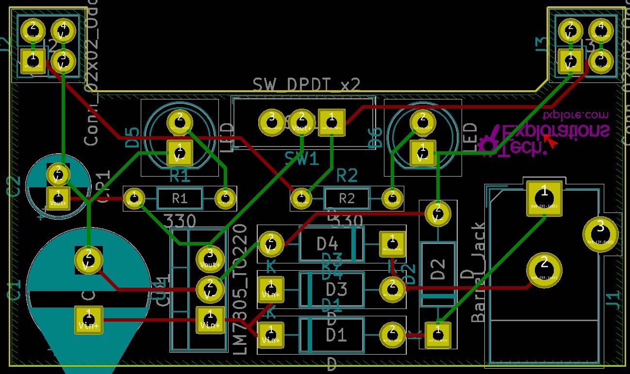
Figure 14.16: The logo footprint has no courtyard defined and triggered the courtyard check.
Because the logo only has silkscreen elements and no electrical or mechanical attributes, you can simply ignore this problem. If this was an actual electrical component, you would need to evaluate it and fixed if you determined that it could affect the operation of the board. Not every warning or problem needs to be dealt with; many can be ignored safely.
Step 8. Manufacturing
The goal of the PCB design process is turning the PCB from a set of files on your computer into a physical object. There are a few ways by which you can do that. At home, you can use a chemical etching process, or a CNC machine to carve out a circuit on a copper board. I personally find the chemical etching process too messy, not to mention that you have to work with potentially toxic chemicals. If you already have a CNC machine, then you can certainly use it to make your boards. With a bit of patience and practice, you will be able to create two, or even four layer boards. In both cases, you will need to use a special process to create vias and holes, with copper-plated holes being more challenging.
I personally prefer the simplicity of using online manufacturers who can produce high-quality boards for a relatively small cost. You will need to plan ahead because the lead time (manufacturing plus shipping) can take a few weeks.
The standard method for ordering a PCB from an online manufacturer is by exporting Gerber files from KiCad and importing them to the manufacturer’s website. Lately, companies like Oshpark make it possible to simply upload Pcbnew’s '.KiCad_pcb' file. I find this development very encouraging because it is so simple. Exporting Gerber files has been the source of many mistakes and wasted time in my life. You have to be careful to export the correct files, with the correct file name extensions and units, and must not forget the drill files. With the ability to upload the '.KiCad_pcb' you automatically eliminate a big risk factor.
In this book, you will learn how to manufacture a PCB with an online service by using both the traditional Gerber files and Pcbnew’s '.KiCad_pcb' file. To learn how to do this, please refer to the relevant recipes in Part 5 of this book (using the KiCad_pcb file and the traditional Gerber files method).
KiCad series
Ready to learn KiCad?

Learn the world's favourite open-source PCB design tool with the world's most comprehensive course
KiCad Like a Pro, 3rd edition is available as a video course or as an eBook.
Choose the version that fits best with your style of learning, or get both to get the full benefit of the video demos plus the details of the eBook.
When you complete KiCad Like a Pro 3e, you'll be able to use KiCad to design and manufacture multi-layer PCBs with highly integrated components and a professional-looking finish.
Work through five projects that give many opportunities to learn and practice all of KiCad's important features.
KiCad Like a Pro 3e contains full sections dedicated to PCB and design principles and concepts. These ensure that you will master the fundamentals so that your PCB project are awesome.
If you are someone who is interested in designing PCBs using KiCad, or moving to KiCad from another CAD application, then KiCad Like a Pro, the video course and eBook, is for you.
We publish fresh content each week. Read how-to's on Arduino, ESP32, KiCad, Node-RED, drones and more. Listen to interviews. Learn about new tech with our comprehensive reviews. Get discount offers for our courses and books. Interact with our community. One email per week, no spam; unsubscribe at any time
