11. Design principles and basic concepts
Schematic Design workflow in Kicad
In a previous article in this series, you learned about the PCB design workflow, without getting into any details. It is time to take a closer look at the two most important parts of the process: the schematic design, and the layout. In KiCad, the schematic design is done using Eeschema, and the layout is done in Pcbnew.
Let’s learn about the workflow of creating a schematic in Eeschema. You can see it in Figure 13.1.
But before we get into it, I’d like to highlight something very important: I designed the workflow that you see in Figure 13.1 to help you take your first few steps in PCB design. As you gain confidence and knowledge, you will develop your own workflow. While you should follow the workflow in Figure 13.1, know that you are by no means 'locked' in it. KiCad is very versatile and can accommodate a huge variety of working styles. It can also work in tandem with other tools in your toolchain, such as other CAD applications, and autoroutes (both of which you will learn about in this book).
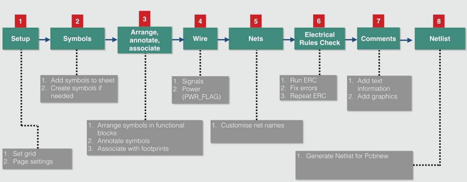
Figure 13.1: The schematic design process.
In addition, engineering and design is a massively iterative process. Linear simply doesn’t work. Yes, the workflow you see in Figure 13.1 is obviously linear, but that’s ok because you will abandon it in favour of an iterative model before you finish working with this book.
Let’s have a look at the 8 steps of the schematic design workflow.
Step 1. Setup
When you start to work on a new schematic in Eeschema, there are two things that you will want to do: configure the grid size and set up the page. The Setup in Eeschema is simpler in that it is in Pcbnew, as you will see.
You can set the grid size from the Display tab of the Schematic Editor Options window, which you can find in the Preference menu (Figure 13.2).
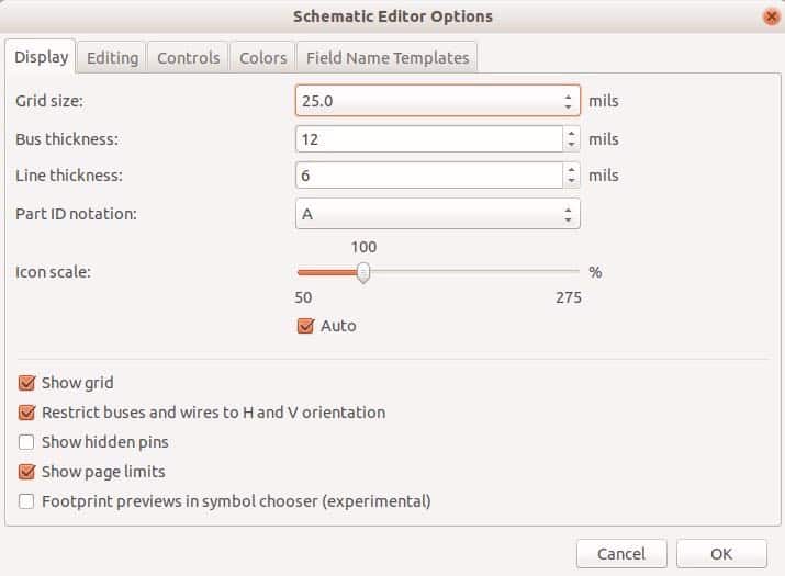
Figure 13.2: You can set the grid size from the Display tab.
The grid size determines where your mouse pointer will snap on the schematic sheet. The snap feature helps in the drawing process so that the end result looks good. The default setting is 25 mils, which I find good for most projects I have worked in.
You should definitely take a few minutes to set up your page in the Page Settings window, available from the File menu (Figure 13.3).
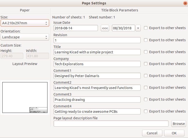
Figure 13.3: The Page Settings window.
Through-hole pads, unlike SMD pads, connect the front for the PCB with the back electrically. In the examples, you can see that the gold plating of the pad fills the inside of the hole. If you turn the PCB around, you will see that a matching pad exists in the back.

Figure 13.3: The Page Settings window.
As in my example in Figure 13.3, you should type in the details of your project, such as the date (you can copy the current date into the field by clicking on the '<<<' button), the revision number and a title. When you print out your schematic (or export it as PDF to share it with others), this information will also be printed. In Pcbnew, you will find the same Page Settings window, as you will see in the next chapter.
Step 2. Symbols
The two most important elements of schematic diagrams are the symbols and the electrical connections between the symbols. The symbols are graphical representations of real-life components. For example, a resistor looks like the symbol in Figure 13.4.
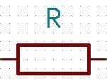
Figure 13.4: The symbol for the resistor.
Assuming you know what you are designing, in the second step of the workflow involves getting all the needed symbols from the symbol chooser and adding them to the schematic sheet (Figure 13.5).
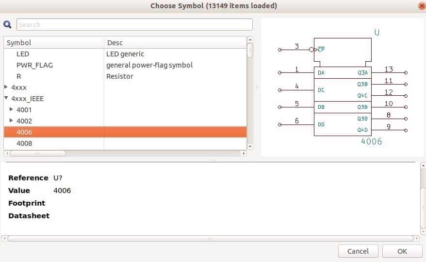
Figure 13.5: Use the symbol chooser to find symbols.
KiCad has a huge variety of symbols and symbol libraries to pick from. On top of that, you can create your own custom symbols and your own libraries. Those custom libraries can contain your custom symbols or symbols that you have collected from other sources.
In this step, simply get all the required symbols on the sheet. If any are missing, create them yourself (you will learn how to do that in this book), or find them by searching on the Internet. Once you have all of them, continue to step 3.
Step 3. Place and annotate symbols
In step 3, you will move the symbols in place, and prepare them for wiring. In Figure 13.6, I have placed the symbols in the approximate position, in relation to the other symbols, so that I can easily wire them in the next step. I want to keep the wires short, with as few angles as possible in order to produce a readable outcome.
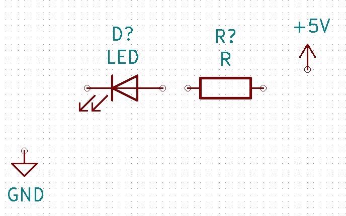
Figure 13.6: Move the symbols in place.
Before you move on to the wiring step (step 4), you should also annotate the symbols. Notice how the LED and the resistor have designators 'D?' and 'R?' in Figure 13.6? The question marks indicate that these symbols have not been annotated. With annotation completed, the schematic will look like the example in Figure 13.7.
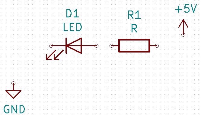
Figure 13.7: The symbols are now annotated.
KiCad can annotate all symbols with the click of a button, as you will see later.
With your schematic symbols annotated, you can move on to Step 4, wiring.
Step 4. Wiring
In step 4, you will connect the symbols using wires. Each wire is attached to a symbol pin and creates a net. In the example of Figure 13.8, the green wires connect the LED and the resistor to the 5V voltage source and the GND. The 5V and GND symbols are special kinds of symbols, 'power' symbols. This schematic contains three wires, so it contains three nets.
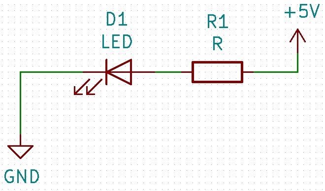
Figure 13.8: The symbols are connected using wires.
Understanding nets is important because of what you can do with them in Pcbnew. The ones in the example here don’t have a custom net name, but they do have an automatically assigned name that Eeschema has generated. With or without a custom net name, this schematic is fully wired, so you can continue in the next step of the workflow, where you will actually assign custom names for these nets, or at least the most important nets.
Step 5. Nets
In step 5 you will name your schematic nets, at least the most important ones. Nets that are important are, for example, those that connect to the GND and 5V symbols. By giving them a custom name to replace the generic one assigned by Eeschema, you will make it easier to work with it in Pcbnew. Typically, power nets are implemented with wider traces to allow them to accommodate higher currents. Other examples of 'important' nets are those that implement antennas, and data or address busses. In either case, the geometry of those nets, once implemented as traces is important, and having a custom name makes their manipulation easier.
The analogy from the world of programming is this: imagine you have a variable that is used as a counter of the number of users participating in a forum discussion. This variable could have any time you like, as long as it is valid. You could call it 'number_or_forum_participants' or 'var32'. Which one would you rather use?
In Figure 13.9 you can see two labels attached to the wires that connect the circuit to the GND and 5V symbols.
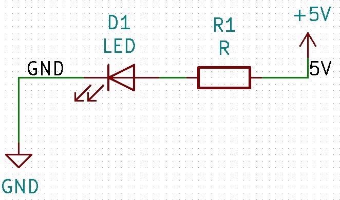
Figure 13.9: This example shows two labeled nets ('GND' and '5V’).
Step 6. Electrical Rules Check
In more realistic circuits than the one with the LED and resistor symbols we have been using as an example, it is a good habit to regularly check for errors. In programming, the equivalent is to regularly run the compiler every time you complete a new segment of code. The compiler will produce messages to draw your attention to defects. You will need to fix those defects before you continue to write new code.
In Eeschema, this kind of check is done by the Electrical Rules Check utility (ERC). The ERC will check for a variety of error conditions, like unconnected pins, problems with power pins, problems with pins connecting to incompatible pins, etc.
In Figure 13.10, the ERC revealed two problems with this schematic. This is one of the most common problems that you will come across to. You learned about this in Part 2, in the section with the title 'Electrical rules check (ERC)'.
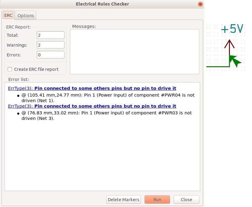
Figure 13.10: This ERC revealed two problems with this schematic.
Step 7. Comments
Let’s continue with the programming analogy. Just like in programming comments are very important to increase the value of your code, similarly, in CAD design and in particular in schematic and layout design, you can use comments for the same purpose. I try to be liberal with comments, especially when I work on schematics and layouts that I plan to share with other people.
Comments come in the form of text labels that highlight features of the schematic, and graphics, such as lines and boxes, that help group segments of the schematic into functional components.
You can see an example in Figure 13.11. I may have gone a bit 'overboard' with my comments, however, the result is that for the reader/learner it is very clear as to what each group of symbols is, and how it relates to the other symbols.
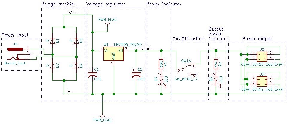
Figure 13.11: This schematic is commented to improve comprehension.
Step 8. Netlist
Your work in the schematic design of your board was complete in Step 7. The only thing left to do in Eeschema is to export the necessary schematic data to Pcbnew, so that you can continue with the layout process. In other CAD applications, a tighter integration between the schematic design and the layout components means that you can jump directly from one to the other. But in KiCad, the two components are separate. To start work on the layout, you need to export the 'netlist' file from Eeschema, and import it into Pcbnew (Figure 13.12).
I find that the separation of the schematic and layout editors in KiCad is a positive design decision. It helps in reinforcing the fact that these two operations are, indeed, separate, and need focus and planning to perform each one well.
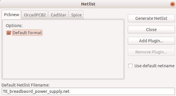
Figure 13.12: Export the netlist from Eeschema prior to starting work on the layout.
The separation between schematic and layout designs means that you must be forward-thinking and disciplined when you are working with the schematic. Imagine that you are working on the layout when you realise that you forgot to place a switch or a pull-up resistor in the schematic. You will have to go back to Eeschema, add the missing symbols, re-export the Netlist, re-import the Netlist to Pcbnew, and start the layout again. If only you had not forgotten in the first place! After a few times of this, I found myself becoming better at thinking ahead and planning during the schematic design work. In turn, this meant fewer iterations, and faster start to end PCB design duration.
Nevertheless, starting with KiCad 5, this overhead is shortened, since a shortcut was introduced by its developers. You can update the netlist from the Pcbnew Tools menu (Figure 13.13).
I still find myself clinging to the old ways of doing things, but I must say that with this shortcut, the integration between Eeschema and Pcbnew is tighter than ever before, without losing the advantages of having separate applications.
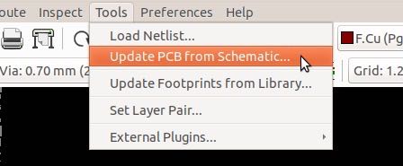
Figure 13.13: Quick import of the netlist into Pcbnew is now possible.
KiCad series
Ready to learn KiCad?

Learn the world's favourite open-source PCB design tool with the world's most comprehensive course
KiCad Like a Pro, 3rd edition is available as a video course or as an eBook.
Choose the version that fits best with your style of learning, or get both to get the full benefit of the video demos plus the details of the eBook.
When you complete KiCad Like a Pro 3e, you'll be able to use KiCad to design and manufacture multi-layer PCBs with highly integrated components and a professional-looking finish.
Work through five projects that give many opportunities to learn and practice all of KiCad's important features.
KiCad Like a Pro 3e contains full sections dedicated to PCB and design principles and concepts. These ensure that you will master the fundamentals so that your PCB project are awesome.
If you are someone who is interested in designing PCBs using KiCad, or moving to KiCad from another CAD application, then KiCad Like a Pro, the video course and eBook, is for you.
We publish fresh content each week. Read how-to's on Arduino, ESP32, KiCad, Node-RED, drones and more. Listen to interviews. Learn about new tech with our comprehensive reviews. Get discount offers for our courses and books. Interact with our community. One email per week, no spam; unsubscribe at any time
