
I’m excited to introduce you to the latest and greatest version of KiCad – version 8 (stable release). This article will overview the new features and capabilities added to this popular open-source electronic design automation (EDA) software.
Whether you’re a seasoned KiCad user or just getting started, it’s important to stay up to date with the latest developments in the software. By reading this article, you’ll better understand the new tools and functionalities available and how they can enhance your design process.
I’ll cover everything from improved user interface enhancements to new functionality streamlining the design process. This article is a must-read to quickly transition to KiCad 8 from a previous version or even a different PCB tool. I last wrote a comprehensive review for KiCad in 2021, for KiCad 6.
KiCad 8 was in development for almost 2023, with three release candidates published in January and February 2024.
So, let’s dive in and explore the exciting new features and capabilities of KiCad 8!
Just in case… What is KiCad?
KiCad is a professional-grade open-source electronic design automation (EDA) software suite that enables the creation of schematics and printed circuit board layouts. It provides comprehensive design, simulation, and manufacturing tools, making it popular among engineers, hobbyists, and students.
KiCad EDA software suite includes a PCB editor for designing printed circuit boards, a schematic editor for creating circuit diagrams, a footprint editor for designing PCB footprints, a symbol editor for designing schematic symbols, and a 3D viewer to inspect the design in a 3D environment. Additionally, it features tools for generating bills of materials (BOM), Gerber files for manufacturing, and support for simulation and project management. I have written an article with more details about the KiCad apps (originally written for KiCad 6, but the core information is still valid).
With its user-friendly interface and a wide range of features, KiCad offers a powerful solution for designing complex electronic projects. Its flexibility, extensive component libraries, and cross-platform compatibility make it a valuable tool for anyone involved in electronics design and engineering.
KiCad competitors
The electronic design industry features several major competitors to KiCad, including Altium, Eagle, and OrCAD.
Altium is known for its user-friendly interface and comprehensive design capabilities, making it a popular choice for professional electronic designers.
Now acquired by Autodesk, Eagle offers a vast library of components and has strong community support, making it a go-to tool for hobbyists and DIY enthusiasts.
On the other hand, OrCAD is well-regarded for its advanced simulation and analysis features, making it a great choice for complex electronic designs.
Each of these competitors boasts unique tools and strengths that can appeal to different segments of the electronic design industry. However, KiCad is open-source and free, making it an accessible option for professionals and hobbyists. Its recent updates and new features further enhance its capabilities and usability in electronic design.
Learn KiCad with my comprehensive
eBook and video course.
Learn more here.
Why use KiCad in a nutshell
KiCad is a valuable tool for electronic schematic design and PCB creation due to its open-source nature, advanced features, lack of board-size restrictions, and ability to generate all necessary files for PCB creation. As an open-source software, KiCad is accessible to anyone who wants it on Windows, Mac OS, and Linux, with professional-level features out of the box and at zero cost.
KiCad is also open and offers the flexibility to customize and adapt the tool to specific needs. Its advanced features, such as 3D rendering and SPICE simulation, make it a powerful option for professional PCB designers who require complex designs and analysis.
Educators can use KiCad to teach students about electronic design and PCB creation, as it provides a comprehensive platform for learning and experimentation. Hobbyists also benefit from KiCad’s user-friendly interface and extensive libraries, allowing them to turn their electronic projects into professional-looking PCBs.
With no restrictions on board size, KiCad is suitable for a broad range of project sizes and complexities.
If you want more reasons to use KiCad, please read my article “Why Learn KiCad“. With the arrival of KiCad 8, these reasons are even stronger, and I can add a few more in an upcoming update of the article.
Overview of KiCad 8’s new features and capabilities
KiCad 8 is the latest version of the world’s most popular open-source electronic design automation software. It was published only a few days ago, on February 23, nearly a year after KiCad 7.
KiCad 8 brings many new features and capabilities to enhance your PCB design process. I will provide details about these improvements later in this article, including brief video demos where possible.
In brief, here are the most notable additions and improvements that come with KiCad 8 (most of the information in this table comes from Jon Evan’s blog post, as well as my own testing):
| Area | Feature | Description |
|---|---|---|
| LIB | Better official KiCad libraries | The KiCad library has added over 1500 symbols and 760 footprints and addressed feedback by introducing a new, intuitive Pin 1 indication style for footprints. |
| PRJ | Improved import tool | KiCad 8 introduces enhanced data import capabilities from various tools, including full projects and libraries, and adds vector graphics support in schematic and symbol editors. |
| PRJ | Improved export tool | KiCad 8 enhances data export capabilities, including PCBs in IPC-2581 format, boards with copper shapes in STEP format for simulations, and schematics in Cadence Allegro format for netlists. |
| PCB | Shape healing | The PCB editor now features shape healing to fix gaps in imported drawings, easing the import of complex shapes. |
| PCB SCH |
Command Line Interface (CLI) | The KiCad CLI, introduced in version 7 and expanded in version 8, now supports DRC/ERC reports in JSON, BOMs, glTF/VRML model exports, layer order control, drawing sheet overrides, and text variable customization, alongside new control flags and bug fixes. |
| ALL | Documentation | KiCad’s Version 8 documentation has been extensively updated. It now covers new features and improvements, with updated screenshots and edits, while translators work on making this information available in more languages. |
| ALL | Hotkeys | You can assign a second hotkey to any action. |
| PCB SCH |
Symbol and footprint previews | The library editors now show a small preview of symbols and footprints when hovering over their names in the library lists |
| SCH | New UI panels for properties, net navigation, and search | KiCad 8’s schematic editor introduces new UI panels, including a properties panel for quick item editing, a search panel for easy navigation, and a net navigator to track nets in complex designs. |
| SCH | New BOM exporter | KiCad version 8 introduces a built-in BOM exporter, enabling in-app customization of data and formatting, including column selection and reordering, with preset saving for future exports. |
| SCH | Pin helpers | Pin Helpers in KiCad’s schematic editor help streamline the creation of labels, wires, and no-connect markers from symbol pins with minimal clicks. |
| SCH PCB |
Symbol and footprint comparison tool | There is a new comparison tool for KiCad that provides a report and visual comparison between the schematic and library versions of symbols and footprints, making it easier to identify differences. |
| SCH | Grid | Grids are better in KiCad 8. The schematic editor’s grid preferences now have overrides allowing different grid settings for specific operations, ensuring consistent alignment, especially for symbols and wires. |
| SCH | Editable power symbols | KiCad 8 now allows power symbols to derive net names from their Value field instead of pin names, enabling custom voltage rails without needing new symbols and aligning closer with other EDA tools. |
| SCH | Named variable fields | KiCad supports special names for custom fields like ${DNP} for symbol properties (e.g., Do Not Place), allowing their export with other fields in a bill of materials. |
| SCH | Item Number | The Symbol Fields Table and BOM Exporter in KiCad now include a new automatic Item Number column, enhancing the organization and tracking of components in the bill of materials. |
| PCB | Arcs | In the updated design tools, users now have the capability to create and modify arcs that extend beyond 180 degrees, allowing for more complex and varied geometric shapes in their projects. |
| SIM | Simulation | KiCad 8 enhances its SPICE simulation tools with a revamped user interface, offering advanced signal plotting, measurements, and four new simulation types. Collaborative efforts with ngspice developers have significantly expanded KiCad’s simulation capabilities, including direct visualization of operating point results on schematics. |
| PCB | Multiple footprint dragging | KiCad 8 expands on the previous version’s capabilities by allowing multiple footprints to be dragged simultaneously with their attached tracks. |
| PCB | Interactive length tuning | KiCad’s length tuning tools in version 8 are revamped, making tuning patterns modifiable objects, thus streamlining design adjustments for controlled-length routing. |
| PCB | Connectivity for graphic shapes | KiCad 8 eliminates the distinction between electrically connected elements and graphical shapes, allowing complex copper geometries to be drawn or imported directly in the board editor, enhancing RF, coil, and sensor design capabilities. |
| PCB | Footprint editor properties pane | The properties panel from the PCB editor has been extended to the library editors in KiCad 8, enabling efficient footprint creation and modification with features like pad size adjustment and mathematical expression evaluation for numeric fields. |
| 3D | 3D Viewer UI | The 3D viewer is updated, aligning its user interface with the PCB editor and adding an appearance panel, visibility presets, and viewports for enhanced control over part and layer visibility. |
| PCB SCH |
Footprint and symbol field sync | Footprints have been enhanced by adding fields synchronized with the fields of their corresponding symbols, ensuring consistency and coherence between the symbol and footprint data within a project. |
| PCB | Ratsnest lines | The feature to customize the thickness of ratsnest lines has been introduced, allowing users to adjust their visibility according to preference. It is particularly useful in enhancing their clarity on densely populated PCB layouts. |
| PCB | Custom-shape pads | The capability to define custom thermal spoke templates for custom-shape pads has been introduced, allowing for greater flexibility and precision in the thermal management of PCB designs tailored to the specific needs of each custom pad shape. |
This table summarises the new and enhanced features of KiCad 8. Let’s take a closer look at each one, starting with a high-level comparison of the user interface in the new KiCad and how it compares against the familiar UI of KiCad 7.
KiCad 7 vs KiCad 8 UI: side-by-side comparison
In this segment, I’ll compare the user interface of KiCad 8 with the user interface of KiCad 7. I’ll look at the individual apps within the KiCad suite and highlight the similarities and differences between the two versions. This comparison will give you a good idea of the changes and improvements made in KiCad 8 and will also serve as a great overview of what to expect from the new version.
I have recorded a detailed video that I invite you to watch. If you prefer to read, continue here.
YouTube video: KiCad 8 UI review
The video and the information in this segment only cover the visible difference between KiCad 7 and 8, as those appear in their user interfaces. I look closely at each new and enhanced feature later in this article.
UI comparison 7 vs 8: Schematic editor
The purpose of the schematic editor in KiCad is to allow users to create and edit schematic designs for electronic circuits. It is an essential tool for electronics engineers and designers to visualize and plan their circuit diagrams before moving on to the PCB layout stage.
Now, let’s dive into the differences and similarities between the KiCad 8 and KiCad 7 schematic editors.

The schematic editor has received much attention with under-the-hood improvements and new features; however, the user interface looks identical at first glance. In the screenshot above, you can notice a new button in the left toolbar (1). When you click this button, the new Properties pane appears to the editor’s left (2). This is a new feature in the schematic editor. However, it was implemented in the layout editor in KiCad 7.
Another new button in the Schematic editor of KiCad 8 allows you to enable grid size overrides for items such as wires, text, graphics and connected items (symbols and their pins). I have marked this button with level “3” in the screenshot above. This grid overdue feature is also present in the symbol editor, the layout editor, and the footprint editor. You can set grid overrides via the KiCad Settings dialogue box (see below). Your grids will work across all your projects, not just those you are working on (it is an application setting, not a project setting).

I have wanted to see this for a long time. With grid override enabled, you can set, for example, a coarse grid for text objects and a fine grid for wires. As you work with these objects, the correct grid is enabled automatically, saving you the trouble of doing this manually. The fast grid switching feature from KiCad 7 is retained.
The rest of the toolbars appear identical. My mouse gestures and keyboard shortcuts operate the same.
UI comparison 7 vs 8: Symbol editor
The purpose of the Symbol editor in KiCad 8 is to allow users to create and modify schematic symbols for use in schematic designs. It provides a user-friendly interface for creating custom schematic symbols and editing existing ones to fit specific project requirements. In this section, I’ll highlight the differences and similarities of the KiCad 8 and KiCad 7 Symbol editor.
In KiCad 8, the Symbol editor has undergone improvements similar to the Schematic editor.

These are two new buttons in the left toolbar: (1) shows and hides the properties manager, and (2) enables and disabled the grid size override. Both buttons work as they do in the Schematic editor.
UI comparison 7 vs 8: Layout editor
The Layout editor in KiCad is the tool we use to design the physical PCB, including the PCB shape, the placement and arrangement of components and route traces, and testing before exporting.
Most of the upgrade work in the Layout editor was done in KiCad 7. In KiCad 8 there is a new button in the left toolbar that controls the grid size overide, as it does in the schematic editor.
I have marked the grid button with the label “1” in the screenshot above. This is, in fact, the only visible difference between the user interface of the layout editor in KiCad 8 and its predecessor in KiCad 7.
However, other improvements in the editor functionality can boost productivity, which I review later. For example, we can now draw arcs that can go beyond 180° and select and drag multiple footprints at once, and there is a better interactive length tuner. I’ll get back to those later.
UI comparison 7 vs 8: Footprint editor
The footprint editor in KiCad 8 creates and modifies custom footprints for electronic components. With this editor, users can design footprints that accurately represent the physical layout of their components, ensuring seamless integration with their PCB designs.
As with the layout editor, there KiCad 8 footprint editor is almost identical to that of KiCad 7.

In the screenshot above, notice the only two additions to the left toolbar: the properties manager (1) and the grid size override switch (2).
Let’s continue with the 3D viewer.
UI comparison 7 vs 8: 3D viewer
The 3D viewer in KiCad 8 is a powerful tool for visualizing PCB designs in a three-dimensional space. It allows you to inspect their designs from all angles, making identifying potential issues and optimising the layout easier.
One significant improvement in KiCad 8 is the reworked user interface of the 3D viewer, which now feels more cohesive with the rest of the PCB editor. Jeff Young’s work on the UI has made it easier for me to navigate and manipulate the 3D model.
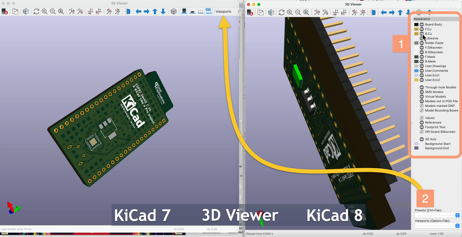
The screenshot above shows the new Appearance pane (1), which works similarly to the Appearance pane in the layout editor. As you enable or disable the elements of the 3D PCB model, those elements appear and disappear in the viewer.
Another change in the UI of the 3D viewer is repositioning the Presents and Viewports dropdown from the top menu bar to the Appearance side panel. I think that this relocation makes sense.
Unfortunately, the raytracing feature, used to add photorealism to a 3D model, is still very slow, even on modern hardware. Because it’s so slow, I rarely use it. Maybe it will receive a speed bump in KiCad 9?
Overall, the 3D viewer is excellent, and the new Appearance pane is another powerful feature.
Import and export
In KiCad 8, there are improvements and updates to the data and project import/export capabilities. Import and export features are crucial for seamlessly integrating projects and collaborating with others. With this latest version, I have found that the import and export functionality has been enhanced to offer a more streamlined and efficient experience.
Let’s look at the details.
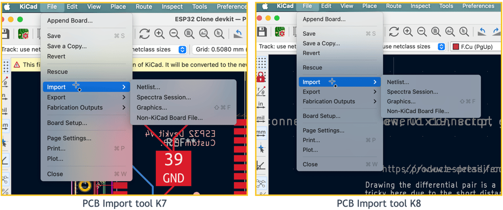
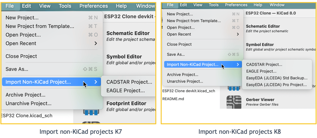
Better support for importing projects from other tools
KiCad 8 introduces a significantly improved project import tool, allowing for importing data and projects from various PCB and CAD tools. This new feature opens up a world of possibilities, making bringing in projects or data from external sources easier than ever.
One of the key highlights is the ability to import PCBs from Solidworks, LTSpice .asc files for schematics, full projects and libraries from EasyEDA Standard and Pro editions, CADSTAR symbol and footprint libraries, and Altium Designer symbol and integrated libraries, as well as EAGLE symbol libraries.
Furthermore, the schematic and symbol editors have been enhanced to support vector graphics import, including DXF and SVG files. This opens up a whole new avenue for annotating designs with custom vector graphics, providing additional options for personalization and customization.
New capabilities for data export
Exporting projects or data is among the most important tools in team or collaborative environments. KiCad users have been able to export project data from the early versions, and in KiCad 8, new export capabilities have been added.
One of the major updates is the support for exporting boards to IPC-2581 format. This format is an all-in-one data package that integrates a board’s fabrication and assembly data, making it easier for users to communicate their designs with manufacturing partners.
In addition, the STEP exporter now has the capability to export copper shapes along with the rest of the board geometry. This is particularly useful for accurate electromagnetic simulation and other applications, providing users with more comprehensive data for their projects.
Below are a couple of screenshots showing the KiCad 7 (left) and KiCad 8 (right) export capabilities from the layout editor.
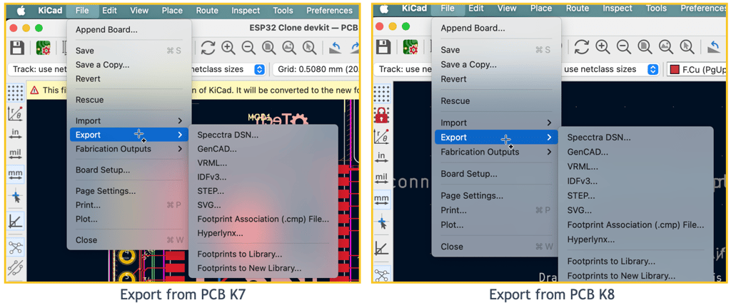
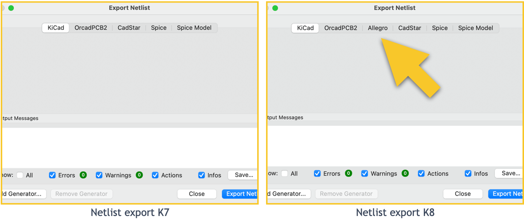
A key highlight is the support for exporting netlists in Cadence Allegro format from the schematic editor. This significant enhancement supports Allegro users who want to utilize KiCad as a schematic capture tool. The screenshot below shows the Netlist export options in KiCad 7 (left) and KiCad 8 (right). As mentioned, KiCad 8 now offers Cadence Allegro as an export option.
Schematic and symbol editor improvements
KiCad 8 introduces several new features and improvements to enhance the user experience and functionality of the software. In the following paragraphs, I’ll explore KiCad 8’s new UI panels, the new BOM (Bill of Materials) exporter, an improved symbol property editor, a new symbol comparator, editable power symbols, new pin helpers, and better net class management and colour coding.
In the schematic editor, you’ll notice a new and improved user interface with customizable UI panels and enhanced navigation for a more intuitive experience. The new BOM exporter makes generating and managing a Bill of Materials easier, streamlining the workflow for creating component lists for your designs. The updated symbol property editor provides a more efficient and user-friendly way to manage symbol properties, making it easier to customize and organize symbols within your designs. Additionally, the new symbol comparator allows easy comparison of symbols, ensuring consistency and accuracy in your designs. Overall, the improvements to the schematic and symbol editor in KiCad 8 offer a more efficient and user-friendly experience for creating and organizing schematics and symbols.
New UI panels
In KiCad 8, the schematic editor has been upgraded by introducing several new UI panels that enhance the user experience. These panels, which can be accessed and toggled via the View menu, offer a range of new capabilities.
One of the most noteworthy additions is the properties panel, which functions similarly to the one found in the PCB editor in KiCad 7. This panel allows for swift editing of the properties of selected items and is now also available in the symbol editor. The properties panel allows you to edit component values without bringing up the component properties pane.
The search panel has also been integrated to provide quick access to search results across large schematics. This feature greatly improves efficiency when navigating through complex designs.
Another notable enhancement is the net navigator, which visually displays the path a highlighted net takes across a complex hierarchical design. This makes it easier to trace and understand the connectivity of components within a schematic.
New BOM exporter
Previously, customizing a bill of materials exported from KiCad required external tools like Python scripts.
KiCad 8 introduces a new BOM exporter. This feature lets users select and reorder columns and format exported BOMs from within the symbol fields table dialogue.
It is more convenient for users to personalize their BOMs. Once an export style is set, it can be saved as a preset.
The new BOM exporter in KiCad 8 provides more flexibility and control, simplifying the process of exporting bills of materials.
Comparison of symbols to library versions
In KiCad 8, a new feature has been introduced to make comparing custom symbols with their original library versions easier. This new comparison tool lets users quickly identify differences between a selected symbol’s schematic and library versions.
This tool was added to address the difficulty in determining the differences between a symbol in the schematic and its library version. This could occur due to local edits to the symbol or updates to the library version after the symbol was placed on the schematic.
Users can now see a report and visual comparison between the selected symbol and its library version with the new comparison tool. This allows for a more efficient and accurate assessment of any discrepancies or changes that may have occurred.
The new symbol comparison tool in KiCad 8 provides users with a valuable tool for ensuring that custom symbols align with their original counterparts in the library. This can help improve the accuracy and consistency of schematics, ultimately contributing to a more streamlined design process.
Editable power symbols
Another improvement in KiCad 8 is the ability to edit power symbols. In previous versions, power symbols like VCC and GND were limited because their net names were based on pin names and could only be renamed in the symbol library editor.
In KiCad 8, this limitation has been addressed. Now, power symbols can take their net name from their Value field rather than their pin name. This means that users can easily create custom voltage rails without creating additional symbols, providing more flexibility and efficiency in the design process.
This enhancement allows for easier customization of power symbols to better suit specific project requirements.
Pin helpers
KiCad 8 introduces a new set of contextual tools in the schematic editor: Pin Helpers.
With just a few clicks, this feature streamlines creating labels, wires, and no-connect markers from symbol pins.
Pin Helpers offers an efficient approach to design by allowing you to add and modify pins directly within the schematic editor easily. Pin Helpers gives you quick access to essential functions for connecting and labelling symbol pins.
PCB and footprint editor enhancements
KiCad 8’s PCB and footprint editors have also received much attention from the developers.
The interactive length tuner has been enhanced, allowing precise control over track lengths. Additionally, users now have the ability to select and drag multiple footprints, streamlining the design process. Another notable improvement is the inclusion of electrically connected graphics shapes, making it possible to create intricate electrically connected copper structures in your PCBs.
The footprint editor has also seen enhancements that mirror those available in the layout editor, resulting in a more cohesive and integrated design experience.
Furthermore, the 3D viewer has been upgraded with an appearance panel, visibility presets, and viewports, allowing for a more dynamic and detailed visualization of the PCB layout.
Let’s look at each one.
Interactive length tuning patterns
KiCad 8 has an improved length-tuning pattern tool. This is part of the PCB editor’s interactive router. This tool allows copper traces to be manipulated after they are placed. This significant improvement greatly speeds up the process of modifying designs with controlled-length routing. This tool works for individual tracks and for differential pairs.
With this update, users can now easily select, modify, and remove tuning patterns, allowing for more flexibility and agility in the design process. This means that any changes needed to control the length or shape of the copper routes can be done quickly within the PCB editor without opening and editing pop-up dialogue boxes.
Multiple footprints select and drag
Another new feature in KiCad 8 is the ability to select and drag multiple footprints simultaneously, along with any attached tracks. In the previous version, KiCad 7, users had the limited ability to drag footprints with tracks attached. In KiCad 8, this capability has been extended to allow for a more efficient and streamlined design process.
With the ability to select and drag multiple footprints and tracks simultaneously, users can adjust their board layout more easily and precisely.
Connectivity for graphic shapes
In KiCad 8, graphic shapes are no longer limited to purely graphical elements. In previous versions of KiCad, these shapes could be drawn on any PCB layer but could not be assigned to a net without creating a footprint and using custom shape pads. However, this restriction has been removed in the latest version.
This means that you now have the flexibility to draw complex copper geometry directly within the board editor and even import copper shapes from external CAD tools.
This capability is particularly useful for RF, coil, and sensor design applications, where intricate copper shapes are essential for optimal performance.
3D Viewer UI overhaul
The 3D Viewer in KiCad 8 has an updated user interface to make it more cohesive with the rest of the PCB editor. One of the most notable additions is the appearance panel, which allows for easier control of the visibility of different types of parts and layers of the board.
For example, you can use the appearance panel to turn on or off individual copper layers, the PCB board body, the silkscreen, the solder paste, or any of the layers in the design. Most technical layers in the PCB editor’s appearance panel are also available in the 3D viewer.
Additionally, the 3D Viewer now includes visibility presets, simplifying toggling between different board views. This can be helpful when presenting or reviewing the design with others.
Another new feature is the introduction of viewports, allowing users to save specific camera positions for quick and easy access.
Ratnest wire size can be customised
In KiCad 8, it is now possible to customize the thickness of ratsnest lines. This allows users to make the ratsnests thicker, making them easier to see in a busy layout.
Simulator
One of the most anticipated updates in KiCad 8 is the improvements to the embedded SPICE simulation tools powered by ngspice. The collaboration between the developers of KiCad and ngspice has resulted in several new features and bug fixes that make circuit simulation more powerful and practical for users.
Ngspice is a mixed-level/mixed-signal electronic circuit simulator. It’s a part of the open-source community, offering a tool for simulating electronic circuits and analysis. Ngspice is based on three open-source software packages: Spice3f5, Cider1b1, and Xspice. It’s widely used for its capabilities in simulating analog and digital circuits, providing detailed analyses of circuit performance, which is crucial for design verification and optimization in the electronics domain.
In KiCad, ngspice integrates with the schematic editor, allowing for circuit simulation directly within the KiCad environment. Users can annotate their schematics with SPICE directives, simulate the circuit, and analyze the results without leaving the KiCad software. This integration streamlines the design process, enabling users to efficiently validate and optimize their circuits.
Whatever circuit you want to simulate (simple circuit, complex circuit, digital, analog, etc.), the simulator will read the circuit schematic from the schematic editor, follow your simulation directives, and run the simulation.
There are two main improvements in the KiCad 8 simulator: an overhauled user interface and four new simulation types. We’ll explore these improvements next.
Simulator UI overhaul
In KiCad 8, the simulator’s user interface was completely overhauled, giving it a more polished and modern look and feel. One of the most exciting new features is the ability to manage plots of multiple signals, allowing for a more comprehensive analysis of circuit behaviour.
Furthermore, the simulator now has the capability to plot power signals in addition to voltage and current, providing a more complete picture of circuit performance.
These updates to the simulator make it an even more powerful tool for circuit design and analysis, offering a more intuitive and efficient user experience.
New simulation features
KiCad 8 introduces four new simulation types that can be configured: pole-zero, noise, S-parameter, and FFT. This expansion in simulation capabilities allows for a more comprehensive and accurate analysis of electronic circuits. Additionally, custom signals can now be defined, enabling the addition of plots for expressions such as V(/in) and V(/out). This enhancement allows for visualising a wider range of simulation outputs directly within KiCad.
Furthermore, operating point simulation results can be visualized directly on the schematic canvas, providing users with a more seamless and intuitive experience. With these new simulation features, users can gain deeper insights into the behaviour and performance of their circuits, making it easier to optimize and refine their designs.
Overall, the new simulation features in KiCad 8 significantly enhance the ability to analyze and visualize simulation data, providing a more robust and efficient workflow for electronic design. These updates reflect KiCad’s commitment to continuously improving and advancing its capabilities to meet the evolving needs of its users.
Other new features in no particular order
KiCad 8 introduces new features and capabilities, further enhancing the user experience and expanding the design possibilities. In addition to the previously mentioned upgrades, there are several other notable new features that I am excited to highlight. These features cover various functionalities, from design improvements to performance enhancements, making KiCad 8 an even more powerful tool for electronic design. In no particular order, let’s explore these additional new features and see how they can benefit designers in their projects.
Net class assignment integration
In KiCad 8, the integration between the schematic and PCB layout has been improved with the automatic reflection of net class assignments. Any net class assignments in the schematic are now seamlessly integrated into the PCB layout, visible in the ‘PCBNew’ environment.
The PCB layout will automatically reflect those changes when you create or modify net classes in the schematic. For example, if you have defined a net class for high-speed signals in the schematic, those signals will be grouped together, and the appropriate design rules will be applied to them in the PCB layout.
This new feature streamlines the design process and ensures that net classes are consistent between the schematic and layout, reducing the potential for errors and mismatches. It also saves time by manually eliminating the need to replicate net class assignments in the schematic and layout.
Hotkey optimization
One of the new features in KiCad 8 is the ability to customize hotkeys for a more streamlined workflow. This capability allows you to assign alternate hotkeys to any action in the schematic and PCB layout views. This means you can set up shortcuts that are most convenient for your personal preferences and work style.
To customize hotkeys in KiCad 8, navigate to the Preferences menu and select Hotkeys. From there, you can assign a second hotkey to any action by clicking on the desired function and entering the alternate key combination.
Teardrop properties
Teardrops in PCB design are small, tadpole-shaped features that improve the reliability of printed circuit boards by enhancing the connection between pads and traces or vias and traces. These additions are particularly useful in high-reliability applications where mechanical stress and thermal expansion might cause pad or cracking. Teardrops help by distributing stress more evenly and reducing the chances of trace detachment under stress. They are often added during the PCB layout phase using design software, which can automatically generate teardrops based on predefined settings.
KiCad 8 now allows you to specify the properties of teardrops for circular and rectangular pads and add teardrops to any pad using the bulk edit feature. You can also use specific teardrops for track-to-track connections.
Improvements to the command-line interface (CLI)
In KiCad version 8, the command-line interface (CLI) has received various new features and capabilities. Now, DRC and ERC can be executed from the CLI, with the ability to generate reports in a machine-readable format (JSON), making integrating with CI (Continuous Integration) pipelines and other similar applications easier. Additionally, Bills of Material (BOMs) can now be exported directly from the CLI, saving time and streamlining the workflow.
Furthermore, the CLI now supports the export of glTF and VRML 3D models, providing more options for sharing and visualization. The order of layers in multi-layer board plots can be controlled, allowing for greater flexibility and customization.
Another useful addition is overriding the drawing sheet when plotting from the command line, giving users more control over their output.
Text variables can also be overridden in the command line, making it possible to customize the value of a text variable as part of a CI pipeline or similar process.
Lastly, existing options gained new control flags, and several bugs were fixed, improving the overall performance and usability of the CLI.
Improvements to documentation
The documentation for KiCad Version 8 has been updated and improved. Many new features and changes are already documented, making it much easier for long-time users to navigate and explore the software.
Not only have the new features been documented, but all areas of the documentation have been improved with updated screenshots, copy editing, and corrections. This ensures that the documentation is clear, accurate, and up-to-date.
In addition, our documentation translators have been hard at work updating the translated text so that users in more languages can have access to the most current KiCad documentation.
Improvements to grid handling
KiCad 8 offers improved grid preferences in the schematic editor by introducing grid overrides. This new feature allows me to force a certain grid when performing operations such as moving or placing objects in the schematic editor.
One of the great things about this feature is that I can switch between different grids for placing text while still keeping symbols and wires on a 50 mil grid to match with the symbol library pin spacing. This level of flexibility in grid handling is a game changer for ensuring precision and consistency in my schematic designs.
I can’t stress enough how much of a time-saver this feature is, as it allows me to seamlessly switch between grids based on the specific needs of my design without having to adjust the grid settings manually each time. And as someone who values efficiency, this is a huge win for me! I’m confident that this enhanced grid handling in KiCad 8 will greatly improve my overall workflow and design accuracy.
Acknowledgements
As I conclude this exploration of KiCad 8, I must extend my sincerest gratitude to everyone involved in bringing this remarkable tool to life. The development and continued enhancement of KiCad is a testament to the dedication and skill of the core team, whose efforts have made KiCad 8 possible and ensured its place as a premier tool for electronics design. Their commitment to excellence and innovation deserves our deepest appreciation.
Equally important are the volunteer developers, whose contributions have enriched KiCad’s features and capabilities. Their willingness to share their expertise and time has significantly impacted KiCad’s growth and utility. I also want to acknowledge the members of the documentation team who provide the essential resources that help users navigate and utilize KiCad effectively. Their detailed guides and tutorials are invaluable to new and experienced users.
I must also thank the KiCad user community, whose feedback and engagement have been crucial in shaping the development of KiCad 8. Your enthusiasm and support are vital to the software’s continuous improvement. Additionally, I appreciate anyone who has submitted a bug report to help refine and enhance KiCad’s stability and functionality.
A special shout-out to the following contributors for delivering the new and updated components of KiCad that I reviewed in this article:
- John Beard and Carsten Presser: Developed a new standard style for Pin 1 indicators on footprints.
- Alex Shvartzkop: Contributed to importing projects and libraries from multiple design tools, improved vector graphics importing, and enhanced PCB editor features, including shape healing and data export enhancements.
- Roberto Fernandez Bautista: Assisted with importing CADSTAR symbol and footprint libraries.
- Jon Evans: Worked on Solidworks PCB board file imports and multiple footprint dragging improvements.
- Chetan Shinde and Jeff Young: Helped with importing LTSpice schematics.
- Seth Hillbrand: Focused on exporting boards to IPC-2581 format.
- Jean-Pierre Charras: Contributed to the STEP exporter for accurate electromagnetic simulation.
- Youbao Zhang and David Schneider: Worked on exporting netlists in Cadence Allegro format.
- Mark Roszko: Enhanced the command-line interface (CLI) with new features.
- Mike Williams: Improved DRC and ERC run from CLI, developed a new BOM exporter, and added pin helpers.
- Graham Keeth: Updated documentation for KiCad 8.
Useful links
Here are some useful links relating to KiCad:
- KiCad project on Gitlab.
- Source code.
- Issues. <– Report bugs here
- Wiki.
- Branches.
- Tags (including for KiCad 8.99)
- KiCad.info (forum)
- Documentation.
- Awesome PCBs made with KiCad.
- My KiCad course 🙂 (getting an update, of course)
What would you like to see in KiCad 9 and beyond?
KiCad 8, the current version of KiCad, brought new features and updates that make the software better so that we can be more productive. The KiCad’s upcoming version 9 is due a year from now, and new versions will come out yearly. What would you like to see in KiCad 9 and subsequent versions?
I invite you to share your ideas for features and enhancements that you believe should be included in future versions to make KiCad the best PCB CAD software.
Whether it’s a small improvement or a groundbreaking feature, your suggestions can help shape the future of KiCad. It could be small, like setting up multiple board files per project. Or a bigger thing, like team collaboration and versioning tools.
Please use the discussion tool below to contribute your ideas and opinions on how we can continue to improve and innovate, ensuring KiCad remains at the forefront of PCB design technology.
Frequently asked questions about KiCad
Who is the owner of KiCad?
KiCad is an open-source project, meaning it is owned and maintained by a community of developers and contributors rather than a single entity. The KiCad project is overseen by the KiCad development team, which consists of individuals who volunteer their time and expertise to improve and enhance the software. Additionally, the project is supported by the KiCad Foundation, a non-profit organization that helps to coordinate and fund development efforts. The ownership structure of KiCad is decentralized, with contributions coming from a diverse range of individuals and organizations in the electronics design community.
Is KiCad better than Altium?
Caveat: I am not an Altium expert and have never used it. What I know about Altium comes from Altium’s website and documentation and reading various discussion threads on the Internet. As a result, I may have misunderstood key aspects of the Altium vs KiCad comparison. If I have, I apologise and ask that you correct me via the discussion tool below this article.
Comparing KiCad and Altium Designer in terms of which is “better” depends largely on the user’s specific needs, budget, and experience level. Both software packages are powerful tools for PCB (Printed Circuit Board) design, but they cater to somewhat different audiences and use cases.
With its comprehensive suite of tools and professional support, Altium Designer is tailored for users who require a more integrated and advanced design process. The learning curve is steeper but for professionals looking to streamline their workflow and leverage cutting-edge features, the investment in time (and subscription fees) can be well worth it.
KiCad, on the other hand, with its open-source nature, not only makes it free to use and encourages a community-driven approach to problem-solving and learning. This can be incredibly empowering, especially for those who enjoy diving into forums and collaborating with others to overcome design challenges.
The cost is perhaps the most stark difference between KiCad and Altium. KiCad’s free, open-source model is incredibly appealing for those on a tight budget or who cannot justify a large investment in software. Altium’s subscription model reflects its professional-grade offering, catering to businesses and professionals for whom the software’s cost is offset by the value it brings to their projects.
Regarding libraries, KiCad is better than Altium for small projects with frequent component changes, allowing for easier management and revision. KiCad also has a more rational and scriptable approach, with Python scripting available out of the box, compared to Altium’s limited scripting capabilities. Additionally, KiCad’s VCS-friendly nature makes tracking changes and collaborating on designs easier.
On the other hand, Altium excels in consistency among multiple designers, thanks to its database library. This allows for schematic symbols, PCB footprints, and 3D models to be linked to a unique part number, ensuring uniformity in design across different users. Altium also offers features like design reuse blocks, which can streamline the design process by automatically adding physical representations to the PCB document during the ECO process.
Ultimately, the choice between KiCad and Altium depends on the project’s specific needs and the designer’s preferences. KiCad may be more suitable for hobbyist projects with frequent changes and a focus on scripting capabilities. At the same time, Altium may be preferred for larger projects requiring consistency and collaboration among multiple designers.
Is KiCad free for commercial use?
Yes, KiCad is free for commercial use. It is licensed under the GNU General Public License (GPL), which means it is open-source and can be used for commercial purposes without licensing fees. Some examples of companies using KiCad include CERN, Arduino LLC, and others contributing to KiCad development efforts.
Is Kicad used professionally?
Yes, KiCad is used professionally by many individuals and companies. While it is often associated with hobbyist projects due to its open-source nature, KiCad has also gained popularity in the professional circuit design industry. Its powerful features, intuitive interface, and continuous development have made it a viable choice for professionals seeking cost-effective and reliable software.
KiCad provides all the essential tools required for professional circuit design, such as schematic capture, PCB layout, and a robust library management system. The software supports multi-sheet schematics, hierarchical design, and offers a wide range of routing options. It also has extensive support for various file formats, including Gerber, ODB++, and STEP, making it compatible with industry standards.
One of the advantages of using KiCad professionally is its active and supportive community. With a vast user base and an extensive online forum, users can easily find answers to their questions, seek guidance, and share knowledge with others in the industry. This active community ensures that KiCad remains up-to-date, with continuous bug fixes, improvements, and the addition of new features.
KiCad Services Corporation, the company behind KiPro, is a leading provider of professional support and services for KiCad EDA. With a team of IPC CID-certified engineers, KiCad Services Corporation offers expert assistance in using KiCad, from basic wiring to high-speed impedance matching. KiPro subscribers can access quick answers to their design and engineering questions and receive help with bug fixes and feature requests. Additionally, KiCad Services Corporation supports advanced features such as hierarchical schematic capture, library management, push and shove routing, real-time 3D rendering, and export production files. For more information about KiCad Services Corporation and its services, visit their website at https://www.kipro-pcb.com/.
Is KiCad used in education?
Yes, KiCad is used in education. Some universities and colleges that use KiCad in their programs include:
- CERN: CERN, the European Organization for Nuclear Research, has significantly supported KiCad and its development. They have used KiCad in various projects and have contributed to its advancement.
- University of Cambridge: The University of Cambridge in the UK has incorporated KiCad into its electronics and engineering programs. University students use KiCad to design printed circuit boards and learn about electronic design automation.
- Oregon State University: Oregon State University in the US has also integrated KiCad into its curriculum. Electrical engineering and computer science students utilize KiCad for PCB design projects and coursework.
- Technical University of Munich: The Technical University of Munich in Germany is another institution that uses KiCad in their engineering programs. Students at the university learn about PCB design and electronic design using KiCad as a tool.
These are just a few examples of universities and colleges incorporating KiCad into their educational programs to teach students about electronic design and PCB layout.
Last updated: March 2, 2024