KiCad 6 Guide series
Overview of the individual KiCad apps
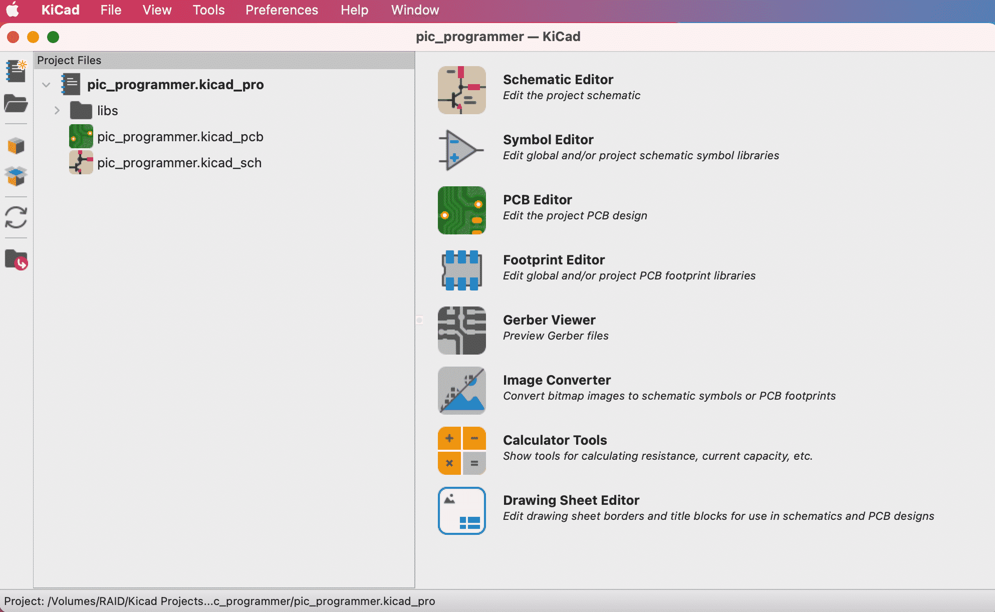
This article will take you on a tour of the individual applications that make up the KiCad software suite.
These are the Schematic, Symbol, Layout (PCB), Footprint, and Drawing Sheet Editors, as well as the Gerber Viewer, the Image Converter, and the Calculator Tools.
Introduction
In the previous article, you learned about the KiCad Project Manager. This article will give you a tour of the individual applications that make up the KiCad software suite.
As you may recall from the previous article, you can access the KiCad applications via the project manager’s right pane or the Tools menu. To open Eeschema or Pcbnew, you can also double-click on the schematic and layout files listed on the middle page of the project manager.
Let’s take a closer look at each of the KiCad applications.
Schematic Editor: Eeschema
Click on the Schematic Editor button to open the application. You can see the editor window below.
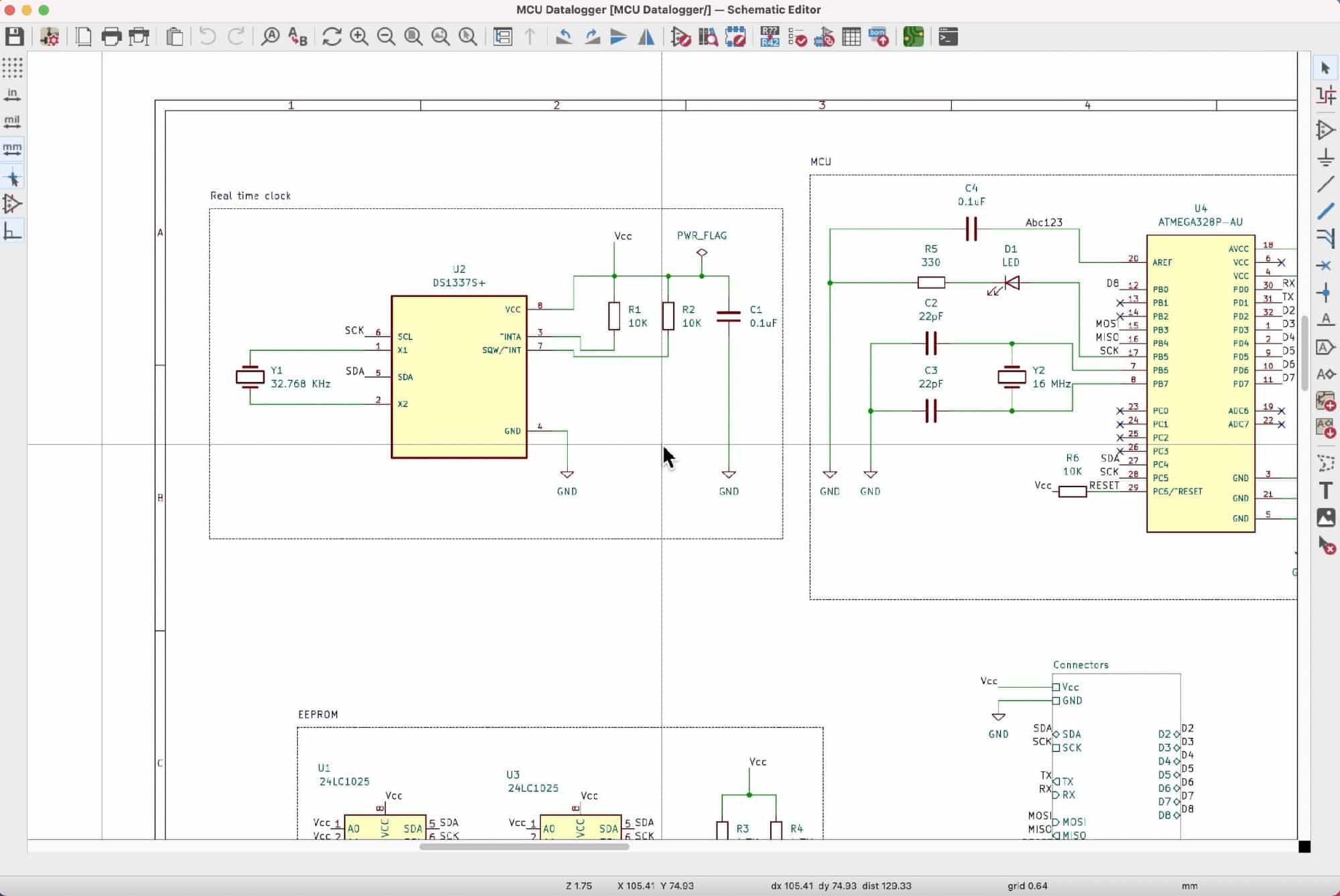
Figure 2.3.1: Eeschema, or the Schematic Editor.
You use Eeschema to draw the schematic of the PCB. Although KiCad is flexible enough and allows you to create PCBs without a schematic, this is rarely a good idea. The schematic diagram captures all necessary information that the layout editor uses: components (as symbols), wires that connect pins, nets, and various kinds of netlabels, busses, power nets, and much more. Eeschema is the first KiCad application you will use when you start a new KiCad project.
In the example above, you can see a schematic from one of the projects in the KiCad Like a Pro 3e course and eBook. You can see the symbols (such as U2, R1, and R2), green wires connecting pins, special symbols representing unconnected pins and power nets, and other elements like graphics and text labels.
You can learn how to use and configure the Schematic Editor in a dedicated part of the course and eBook.
Layout (PCB) Editor: Pcbnew
Once you have completed work in Eeschema, you will continue with the Layout Editor, or “Pcbnew.” To open Pcbnew, you can click on the Pcbnew button in the KiCad project manager or the Pcbnew button in the top toolbar of Eeschema. Below you can see an example instance of Pcbnew.
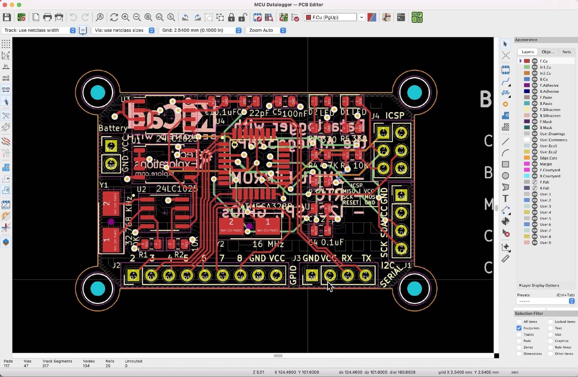
Figure 2.3.2: Pcbnew, or the Layout Editor.
In the example above, you can see the finished PCB design from one of the projects in this guide. The Layout Editor allows you to select the layers and design elements you want to see. For example, you can enable or disable the visibility of layers, footprints, tracks, zones, and vias. In the example above, I have enabled the visibility of all layers and elements and an outline of the top and bottom copper zones.
The Layout Editor includes various sophisticated tools, such as an interactive router and a 3D viewer. You can see a 3D rendering of the PCB from Figure Figure 2.3.2 below:
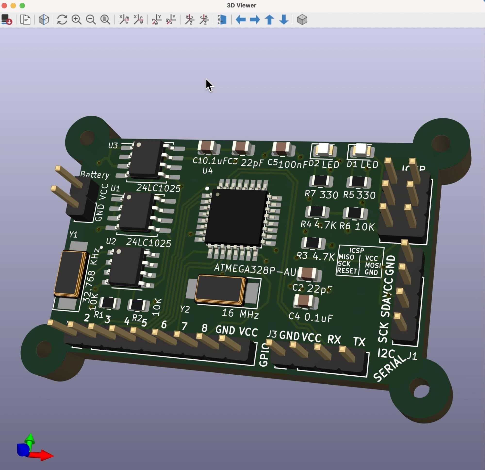
Figure 2.3.3: The 3D viewer in Pcbnew.
You can learn how to use and configure the layout editor in a dedicated Part of this guide.
Symbol Editor
Let’s continue with the Symbol Editor. You can open this application from the KiCad Project Manager or the top toolbar of Eeschema.
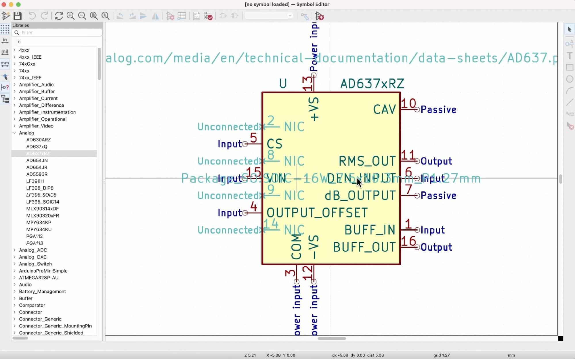
Figure 2.3.4: The Symbol Editor.
With the Symbol Editor, you can modify existing symbols or create new ones. You can think of the Symbol Editor as a simplified version of the schematic editor. In the Symbol Editor, you can work with a single symbol at a time.
KiCad 6 comes with an extensive set of symbol and footprint libraries. There are also thousands of third-party symbols and footprints that you can import. However, you will eventually need to create a symbol, and that’s when the Symbol Editor comes in.
You can learn how to create new symbols from scratch with the KiCad like a Pro 3e course or eBook.
Footprint Editor
Similar to the symbol editor, there is also the Footprint Editor. You can open the Footprint Editor from the KiCad project window or the Pcbnew top toolbar.
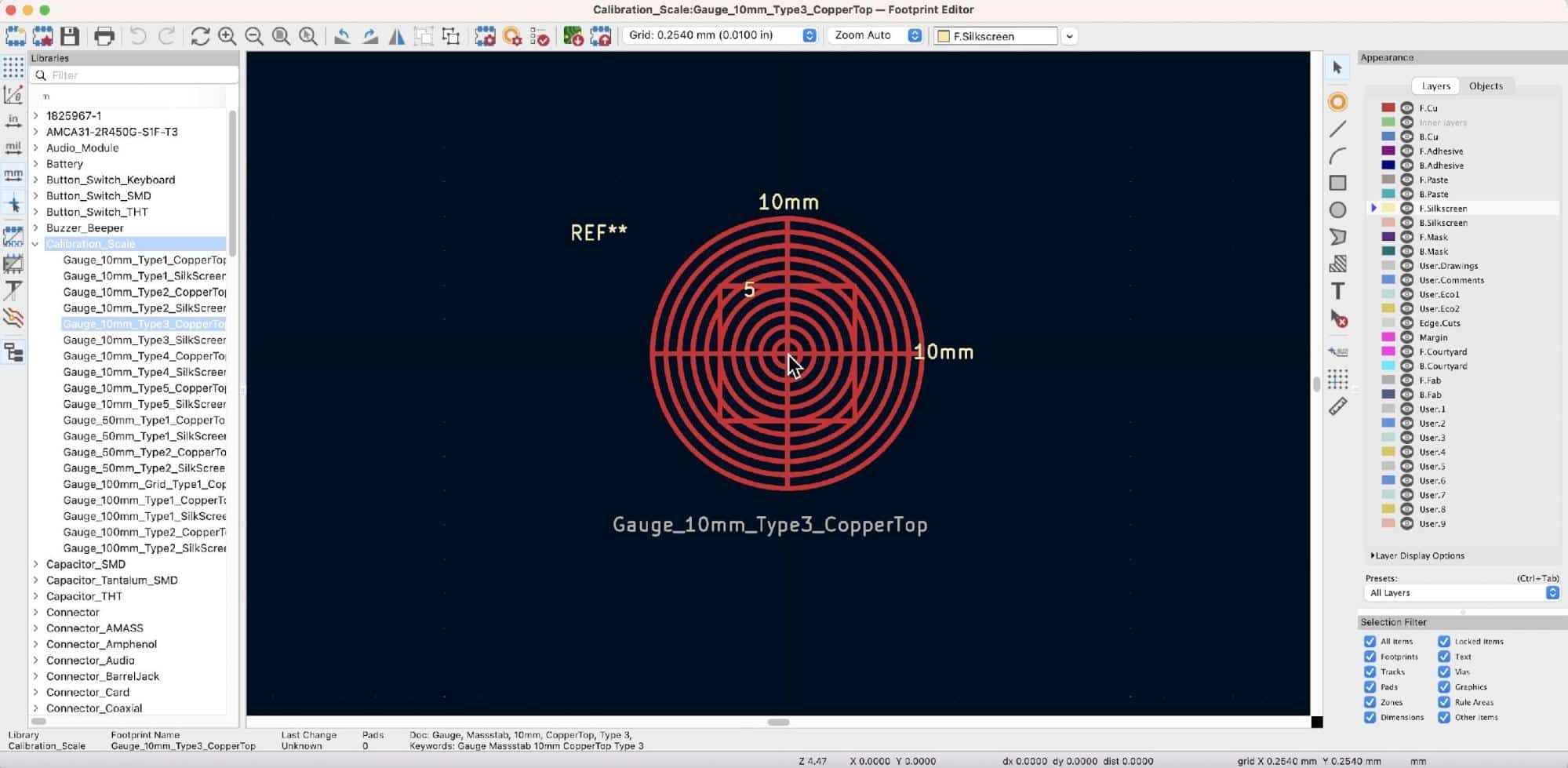
Figure 2.3.5: The Footprint Editor.
With the Footprint Editor, you can create a footprint from scratch or modify an existing footprint. The Footprint Editor also contains a wizard that allows you to quickly generate footprints that follow convention, such as those that use BGA, QFN, DIP and SOIC, packages.
You can learn how to use the footprint editor in a dedicated part of the KiCad like a Pro 3e course or eBook.
Gerber Viewer
When you have completed work on your PCB and wish to order it from an online manufacturer, the most common way is to export a set of Gerber files from Pcbnew. Before you upload those files to your preferred manufacturer, you should take the time to inspect them. KiCad has a tool for this: the Gerber Viewer.
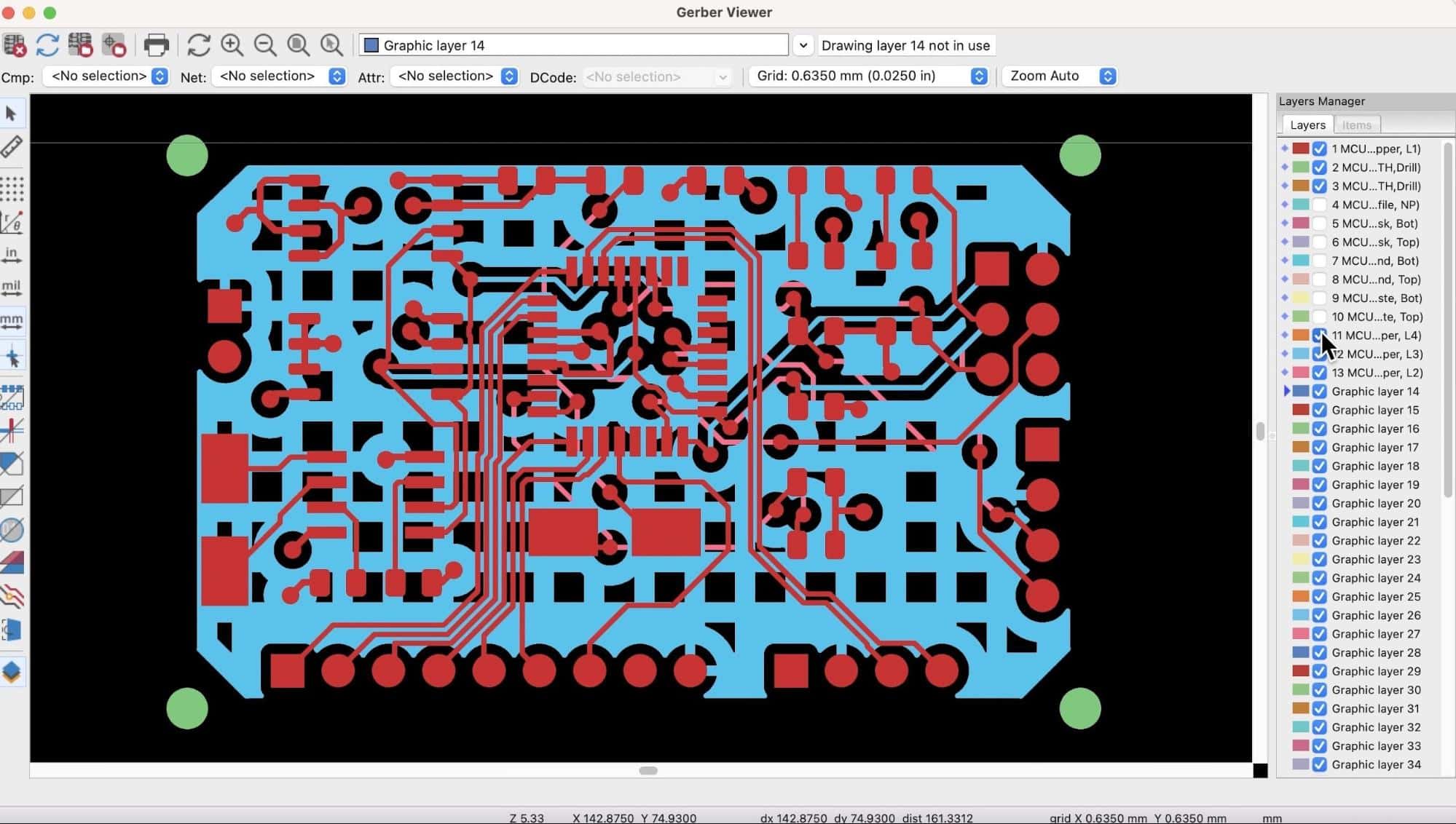
Figure 2.3.6: The Gerber Viewer.
With the Gerber Viewer, you can examine the project Gerber files visually, layer by layer. This way, you can ensure that all its elements are correct. Silkscreen text and graphics, drills, copper fills, the board outline, and cutouts, etc.
Think of the Gerber Viewer as a quality control tool. Use it to reduce or eliminate the risk of ordering a defective PCB.
You can learn how to export the Gerber files and use the Gerber Viewer (and online Gerber viewers) in dedicated parts of the KiCad like a Pro 3e course and eBook.
Image Converter
You can open the Image Converter app from the KiCad Project Manager. With the Image Converter, you can convert a bitmap image into a footprint. Typical uses of the converter are to create a graphics footprint (such as a company logo) or a footprint with an irregular shape that would be too tedious to design in the footprint editor.
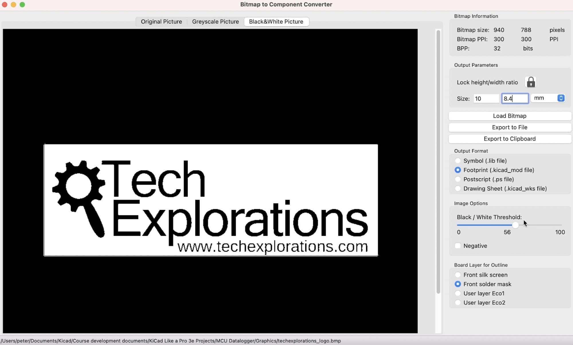
Figure 2.3.7: The Image Converter.
In the example above, I use the Image Converter to create a logo that I can include in my PCBs. You can learn how to use the Image Converter in a dedicated part of the KiCad like a Pro 3e course and eBook.
Calculator Tools
The Calculator Tools contain multiple calculators. Here is a list of tools:
- Voltage regulators.
- RF Attenuators.
- E-Series.
- Resistor color codes.
- Transmission lines.
- Via size.
- Track Width.
- Electrical spacing.
- Board classes.
In the example below, I am using the Track Width calculator to calculate the correct width given a set of parameters.
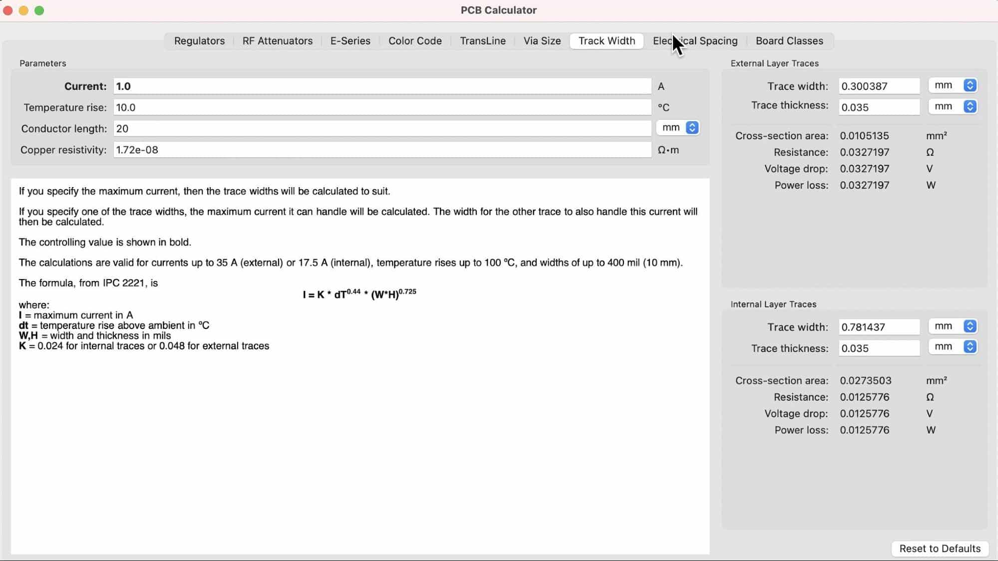
Figure 2.3.8: The Calculator Tools.
You can learn how to use the Track Width calculator by going through the relevant lectures or chapters in the Recipes part of the KiCad like a Pro 3e course or eBook. The mode of operation for the rest of the calculators is similar.
Drawing Sheet Editor
The last main application in the KiCad suite is the Drawing Sheet Editor. You can use this editor to customize your schematic editor sheet. You can see the editor in the example below.
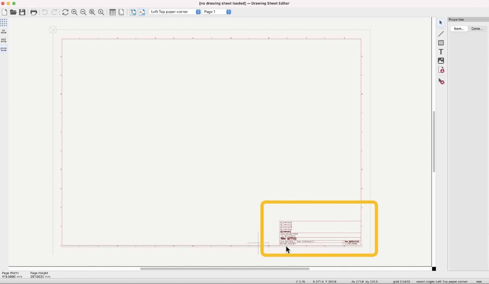
Figure 2.3.9: The Drawing Sheet editor.
With the Drawing Sheet Editor, you can change the size of the schematic sheet and everything within it. For example, you can remove or change the size and location of the information container. You can also change the setup of the text placeholders inside the information box.
To learn how to use the Drawing Sheet Editor, please go through the relevant material of the KiCad like a Pro 3e course or eBook.
Ready to learn KiCad?

Learn the world's favourite open-source PCB design tool with the world's most comprehensive course
KiCad Like a Pro, is available as a video course or as an eBook.
Choose the version that fits best with your style of learning, or get both to get the full benefit of the video demos plus the details of the eBook.
When you complete KiCad Like a Pro, you'll be able to use KiCad to design and manufacture multi-layer PCBs with highly integrated components and a professional-looking finish.
Work through five projects that give many opportunities to learn and practice all of KiCad's important features.
KiCad Like a Pro contains full sections dedicated to PCB and design principles and concepts. These ensure that you will master the fundamentals so that your PCB project are awesome.
If you are someone who is interested in designing PCBs using KiCad, or moving to KiCad from another CAD application, then KiCad Like a Pro, the video course and eBook, is for you.
Jump to another article
KiCad 6 Guides
0. Why learn KiCad?
1. What is a PCB?
2. The PCB design process
3. PCB fabrication
4. Get KiCad for your operating system
5. An example KiCad project
6. KiCad Project Manager (main window)
7. Overview of the individual KiCad apps
8. KiCad Paths and Libraries
9. Create a new KiCad project from scratch
10. Create a new KiCad project from a template
11. KiCad 6 on Mac OS, Linux, and Windows
12. Major differences between KiCad 6.0 and 5.0
13. KiCad Schematic symbols
14. PCB key terms
Contributed articles
Last Updated 1 year ago.
We publish fresh content each week. Read how-to's on Arduino, ESP32, KiCad, Node-RED, drones and more. Listen to interviews. Learn about new tech with our comprehensive reviews. Get discount offers for our courses and books. Interact with our community. One email per week, no spam; unsubscribe at any time
