3. Introduction to KiCad
The PCB design process
To design a printed circuit board, you have to complete several steps, make decisions, and iterate until you are satisfied with the result. Because you are creating something that must be able to perform a specific operation (or multiple operations) well, your design work must be of high quality, safe, and manufacturable. There is no point designing a PCB that can’t be manufactured.
Apart from the practical considerations of designing a PCB, there are also the aesthetic ones. You want your work to look good, not just to function well. Designing a PCB, apart from being an engineering discipline, is also a form of art.
In this book, you will learn about the technical elements of designing a PCB in KiCad, but I am sure that as you start creating your PCBs, your artistic side will emerge. Over time, your PCB will start to look uniquely yours.
PCB design is concerned with the process of creating the plans for a printed circuit board. It is different from PCB manufacturing. In PCB design, you learn about the tools, process, and guidelines useful for creating such plans. In PCB manufacturing, on the other hand, you are concerned about the process of converting the plans of a PCB into the actual PCB.
As a designer of printed circuit boards, it is useful to know a few things about PCB manufacturing, though you surely do not need to be an expert. You need to know about the capabilities of a PCB manufacturing facility so that you can ensure that your design does not exceed those capabilities and that your PCBs are manufacturable. PCB manufacturers will supply “design rules” which specify the dimensions and tolerances they can meet. For example, they may require that all traces be a minimum of 5 thousandths of an inch wide.
As a designer, you need to have an understanding of the design process, and the design tools. To want to design PCB, I assume that you already have a working knowledge of electronics. Designing a PCB, like much else in engineering, is a procedural and iterative process that contains a significant element of personal choice. As you build up your experience and skills, you will develop your unique designing style and process.
While a personalised design process contains unique elements, it still follows the generic process you will learn about in this book. I distilled this process by drawing from my own experience and learning from other people’s best practices. I also tried to simplify this process and make it suitable for people new to PCB design.
The Kicad design workflow
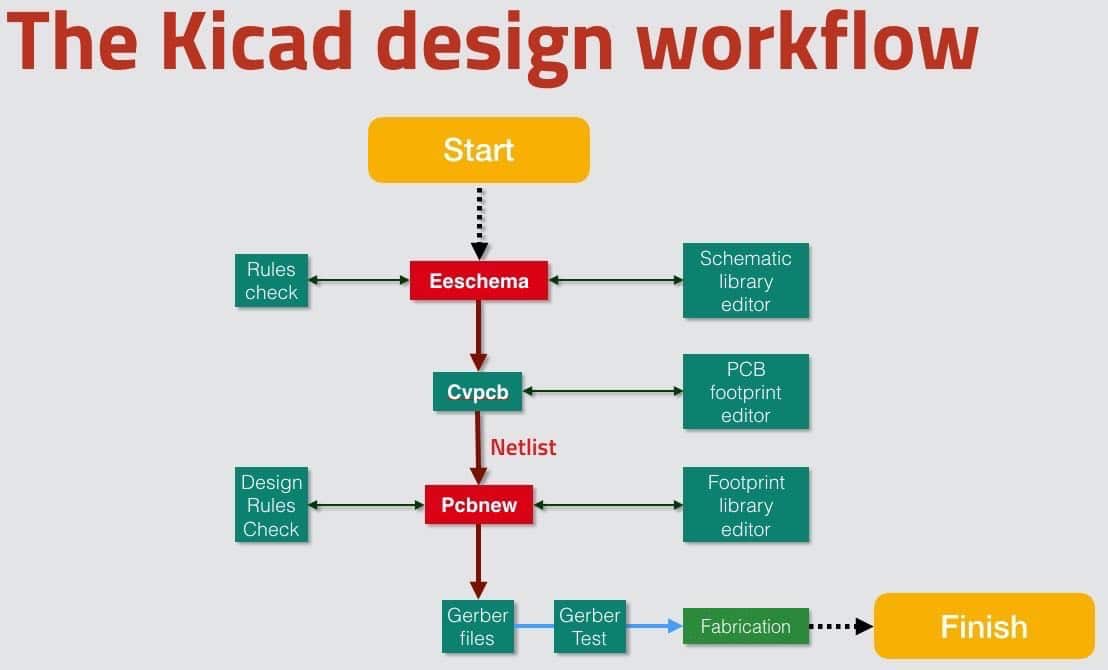
Since, in this guide, book and course, you will be using KiCad, I have created a schematic that shows the PCB design process using KiCad terms and tools. You can see it in Figure 2.1.

Figure 2.1: The KiCad design workflow.
From a very high-level perspective, the PCB design process only has two major steps:
1. it starts with a schematic diagram;
2. it ends with the layout.
The goal of the design is to create the layout. The layout is a file that contains information about your board, which the manufacturer can use to create the board. The layout must contain information about the size and shape of the board; its construction (such as how many layers it must have); the location of the components on the board, the location of various board elements, like pads, holes, traces and cutouts; the features of these elements (such as the sizes of holes and traces); and much more (which you will learn in detail later in this book).
When we bring this generic process to KiCad, we can map it to the elements that you see in Figure 2.1.
Eeschema, the schematic design editor
The process begins with Eeschema. In Eeschema you create the electrical schematic that describes the circuit that eventually will be manufactured into the PCB. You draw the schematic by selecting symbols from the library and adding them to the schematic sheet. If a component that you need doesn’t exist in the library, you can create it using the schematic library editor.
Running regular electrical rules checks helps to detect defects early. Eeschema has a built-in checker utility for this purpose, as has Pcbnew, the layout editor. These utilities help to produce PCBs that have a low risk to contain design or electrical defects.
There are two things that you need to do before we go to Pcbnew:
1. associate the components in Eeschema with footprints;
2. create the netlist file, which contains information that Pcbnew needs to set up the layout sheet. The netlist file is what connects Eeschema and Pcbnew.
A symbol is a graphical representation of a real component in the schematic; it does not have a physical counterpart. However, in the layout editor (Pcbnew), everything is real in the sense that it has a real-world counterpart. Therefore, you, as the designer, must associate the symbol with a footprint. The footprint is a real thing; it represents resistors, switches, and pads on the PCB. This allows us to match schematic components with footprint modules.[3]
Netlist
Once you have created the associations between symbols and modules, you will then export the Netlist file from Eeschema. Then, you’ll import the netlist into Pcbnew, and all the footprints that you associated in Eeschema will appear in a new sheet so you can start working on the layout.
Pcbnew, the layout editor
You use Pcbnew to position the footprints on the sheet and wire them. Wiring can be very time-consuming, especially for large boards. It is possible to use tools that do the wiring automatically, a capability that can significantly reduce the layout time.
Once you have your PCB laid out and have its traces completed, you can go ahead and do the design rules check. This check looks for defects in the board, such as a trace that is too close to a pad or two footprints overlapping.
Note that different PCB manufacturers may have different capabilities, and/or they may offer enhanced capabilities for a higher price. If you are designing a complex board with densely packed components, you may want to shop around to find a manufacturer with suitable design rules for your needs.
When you are finished working on the layout, you can continue with the last step which involves exporting the layout information in a format that is compatible with your board manufacturer’s requirement. The industry standard for this is a format called ‘Gerber.’ Gerber files contain several related files, with one Gerber file per layer on your PCB, and contain instructions that the fabrication house needs to manufacture your PCB.
Let’s move on to the next chapter where we’ll talk about fabrication.
Notes
[3] In KiCad, a schematic contains symbols, and a layout contains footprints.
KiCad series
Ready to learn KiCad?

Learn the world's favourite open-source PCB design tool with the world's most comprehensive course
KiCad Like a Pro, is available as a video course or as an eBook.
Choose the version that fits best with your style of learning, or get both to get the full benefit of the video demos plus the details of the eBook.
When you complete KiCad Like a Pro, you'll be able to use KiCad to design and manufacture multi-layer PCBs with highly integrated components and a professional-looking finish.
Work through five projects that give many opportunities to learn and practice all of KiCad's important features.
KiCad Like a Pro contains full sections dedicated to PCB and design principles and concepts. These ensure that you will master the fundamentals so that your PCB project are awesome.
If you are someone who is interested in designing PCBs using KiCad, or moving to KiCad from another CAD application, then KiCad Like a Pro, the video course and eBook, is for you.
Jump to another article in this series.
Last Updated 4 years ago.
We publish fresh content each week. Read how-to's on Arduino, ESP32, KiCad, Node-RED, drones and more. Listen to interviews. Learn about new tech with our comprehensive reviews. Get discount offers for our courses and books. Interact with our community. One email per week, no spam; unsubscribe at any time
