2. Introduction to KiCad
What is a Printed Circuit Board?
As a child, I remember my interest in electronics grew, from admiration of what these smart engineers had come up with, to curiosity about how these things worked. This curiosity led me to use an old screwdriver that my dad had left in a drawer (probably after fixing the hinges on a door), to open anything electronic with a screw large enough for the screwdriver to fit in.
A record player, a VCR, a radio: All became my victims. I am still amazed that a charged capacitor didn't electrocute me. At least, I had the good sense to unplug the appliances from the mains. Inside those devices, I found all sorts of amazing things: resistors, transformers, integrated circuits, displays.
All of those things were fitted on small boards, like the one in Figure 1.1. This is an example of a printed circuit board, or PCB, for short.
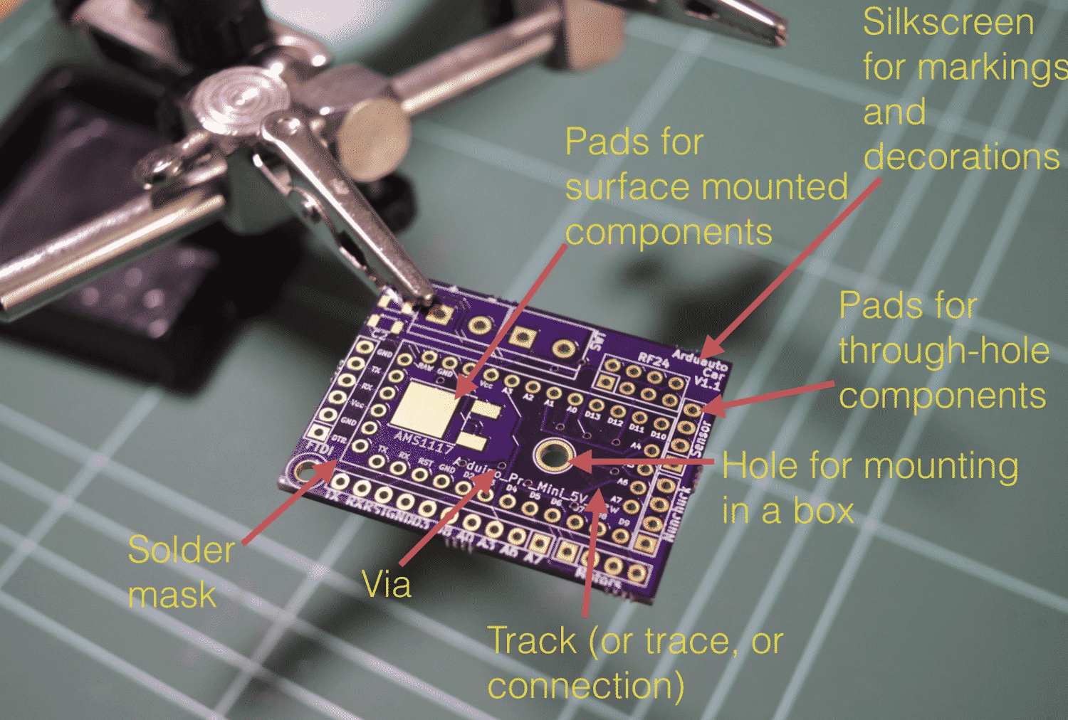
Figure 1.1: The top side of a printed circuit board.
Let's have a look at the components of a PCB, what a PCB looks like, and the terminology that we use. The example PCB is one I made for one of my courses (Figure 1.1).
Elements of a PCB
The top side of the PCB is the side where we place the components. We can place components on the bottom side, too; however, this is unusual.
Components
In general, there are two kinds of components: through-hole or surface-mounted components. Through-hole components are attached to the PCB via inserting the leads or the pins through small holes and using hot solder to hold them in place. In the example pictured in Figure 1.1, you can see several holes into which you can insert the through-hole component pins. The holes extend from the top side to the bottom side of the PCB. They are plated with a conductive material, such as tin, or in this case, gold. We use solder to attach and secure a component through its lead onto the pad that is surrounding the hole (Figure 1.1).
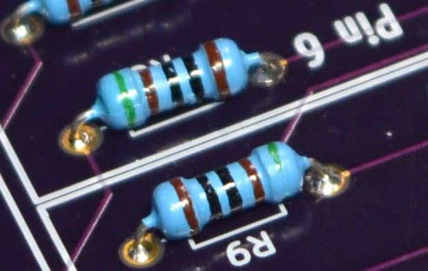
Figure 1.1: A through-hole component attached to a PCB.
If you wish to attach a surface-mounted component, then instead of holes, you attach the component onto the surface of the PCB using tin-plated pads. You will use just enough solder to create a solid connection between the flat connector of the component and the flat pad on the PCB (Figure 1.2).
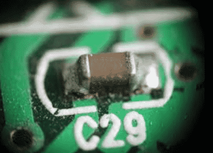
Figure 1.2: A surface-mounted component attached to a PCB.
Silkscreen
Next is the silkscreen. We use the silkscreen for adding text and graphics. The text can provide useful information about the board and its components. The graphics can include logos, other decorations, and useful markings.
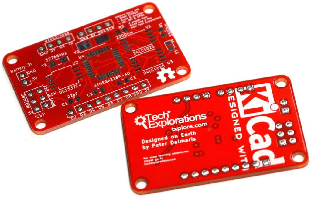
Figure 1.3: The white letters and lines is the silkscreen print on this PCB.
In Figure 1.3, you can see that I've used white boxes to indicate the location of various components. I've used text to indicate the names of the various pins, and I've got version numbers up there. It's a good habit to have a name for the PCB and things of that sort. Silkscreen goes on the top or the bottom of the PCB.
Mounting holes
Sometimes, you may want to secure your PCB onto a surface. To do that, you can add a mounting hole. Mounting holes are similar to the other holes in this board, except that they don't need to be tinned. You can use a screw and a nut and bolt to the other side so that the PCB is secured inside, for example, a box.
Tracks and traces
Next are the tracks. In this example (Figure 1.4), they look red because of the color of the masking chemical used by the manufacturer.
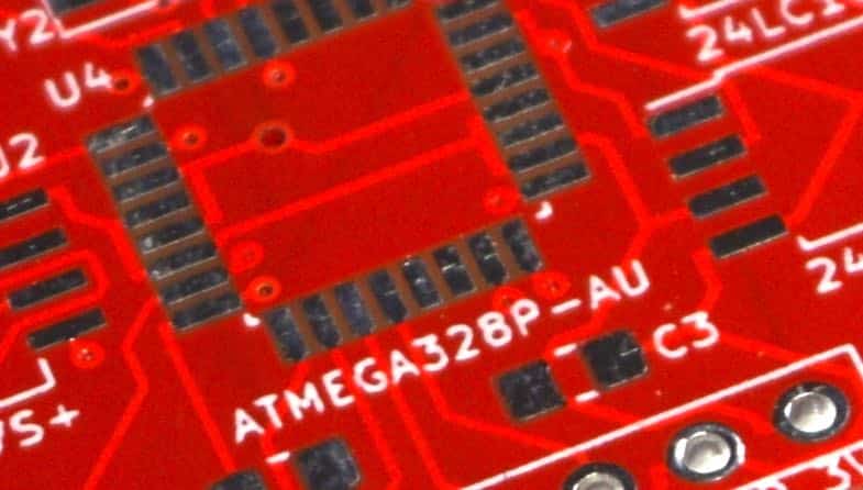
Figure 1.4: The bright red lines connecting the holes are tracks.
Tracks are made of copper, and they electrically connect pins or different parts of the board. You can control the thickness of a track in your design. Tracks can also be referred to as ‘traces.’
Vias
Notice the small holes that have no pad around them? These are called ‘vias.’ A via looks like a hole but is not meant to be used to mount a component on it. A via is used to allow a track to continue its route to a different layer. If you’re using PCBs that have two or more layers, then you can use vias to connect a track from any one of the layers to any of the other layers. Vias are very useful for routing your tracks around the PCB.
Soldermask
The red substance that you see on the PCB is the solder mask. It does a couple of things. It prevents the copper on the PCB from being oxidized over time. The oxidization of the copper tracks negatively affects their conductivity. The solder mask prevents oxidization.
Another thing that the solder mask does is to make it easier to solder by hand. Because pads can be very close to each other, soldering would be very difficult without the solder mask. The solder mask prevents hot solder from creating bridges between pads because it prevents it from sticking on the board. (Figure 1.5). The solder mask prevents bridges because solder cannot bond with it.
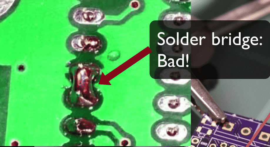
Figure 1.5: A solder bridge like this one is a defect that solder mask helps in preventing.
Often, the tip of the solder, the soldering iron is almost as big or sometimes as bigger than the width of the pads, so creating bridges in those circumstances is very easy and solder mask helps in preventing that from happening.
Materials
In Figure 1.6, you can see an example of the standard 1.6mm thick PCB.
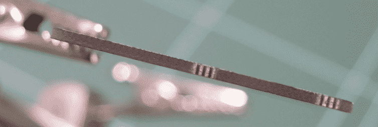
Figure 1.6: This PCB has a thickness of 1.6mm, and is made of fiberglass.
Typically, PCBs are made of fiberglass. The typical thickness of the PCB is 1.6 millimeters. In this close-up view of a PCB picture (Figure 1.7), you can see the holes for the through-hole components. The holes for the through-hole components are the larger ones along the edge of the PCB. Notice that they are tined in the inside, electrically connecting the front and back.
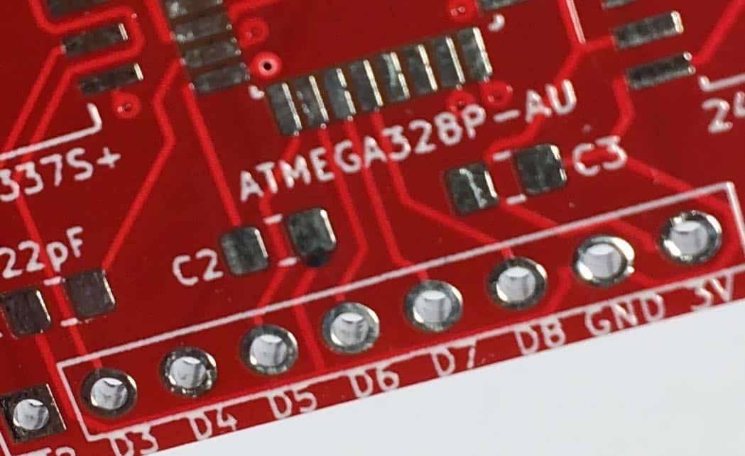
Figure 1.7: A closeup view of the top-layer.
In Figure 1.7, you can see several vias (the small holes) and tracks, the red solder mask, and the solder mask between the pads. In this close up, you can also see the detail of the silkscreens. The white ink is what you use in the silkscreen to create the text and graphics.
Figure 1.8 is interesting because it shows you a way to connect grounds and VCC pads to large areas of copper, which is called the copper fill.
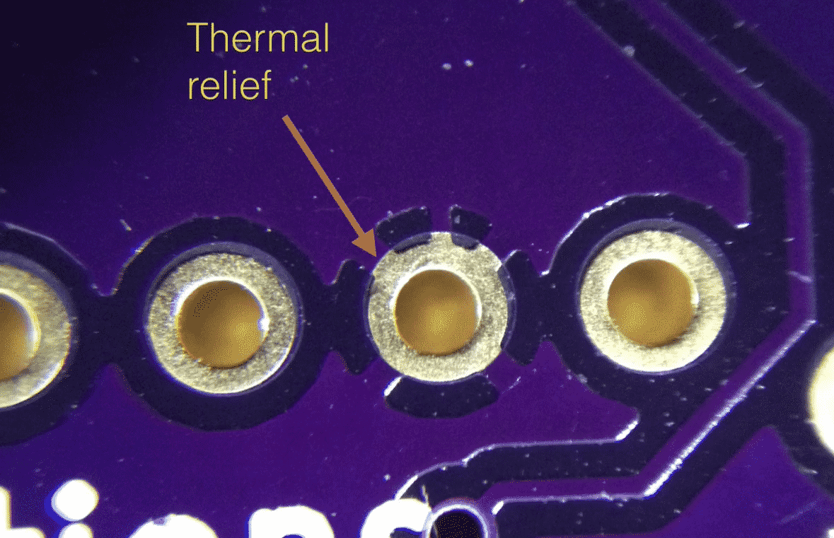
Figure 1.8: Thermal relief connects a pad to a copper region.
Also good to know
In Figure 1.8, the arrow points to a short segment of copper that connects the pad to a large area of copper around it. We refer to this short segment of copper as a ‘thermal relief.’ Thermal reliefs make it easier to solder because the soldering heat won’t be dissipated into the large copper area.
Figure 1.9 gives a different perspective that allows appreciating the thickness of the tracks.
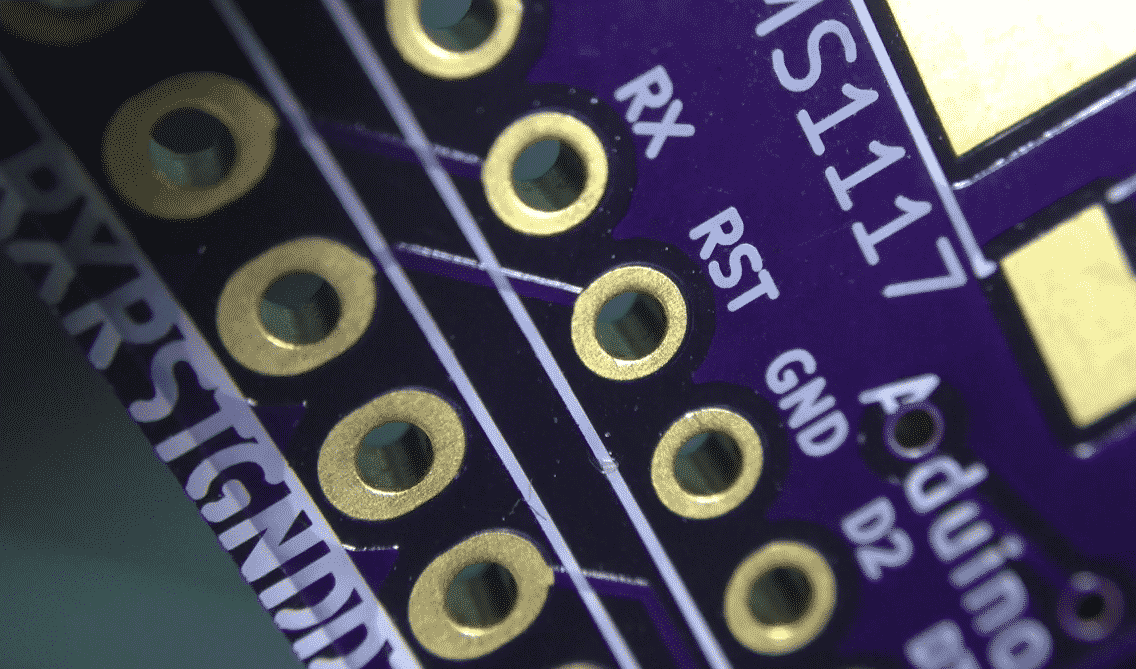
Figure 1.9: The plating of the holes covers the inside of the hole, and connects that front end with the back end.
Notice the short track that connects the two reset holes (RST)? The light that reflects off the track's side gives you an idea of that copper's thickness, which is covered by the purple solder mask.
You can also see a very thin gold layer covering the hole and the pad, and how that fills the inside of the hole. This is how you electrically have both sides of the hole connected.
Instead of gold plating, you can also use tin plating to reduce the manufacturing costs.
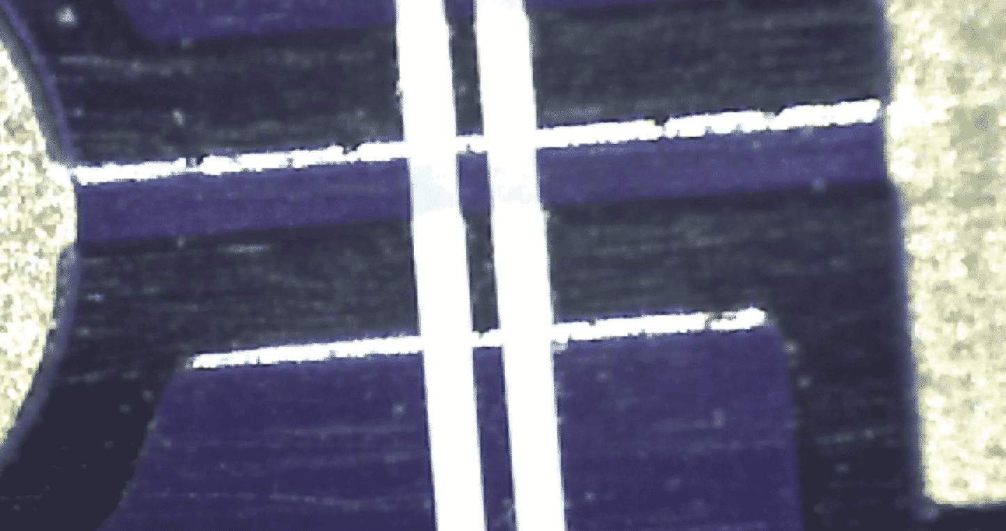
Figure 1.10: A detail of this example board at 200 times magnification.
The image in Figure 1.10 is at 200 times magnification. You can see a track that connects two pads and the light that reflects off one side of the track.
KiCad series
Ready to learn KiCad?

Learn the world's favourite open-source PCB design tool with the world's most comprehensive course
KiCad Like a Pro, is available as a video course or as an eBook.
Choose the version that fits best with your style of learning, or get both to get the full benefit of the video demos plus the details of the eBook.
When you complete KiCad Like a Pro, you'll be able to use KiCad to design and manufacture multi-layer PCBs with highly integrated components and a professional-looking finish.
Work through five projects that give many opportunities to learn and practice all of KiCad's important features.
KiCad Like a Pro contains full sections dedicated to PCB and design principles and concepts. These ensure that you will master the fundamentals so that your PCB project are awesome.
If you are someone who is interested in designing PCBs using KiCad, or moving to KiCad from another CAD application, then KiCad Like a Pro, the video course and eBook, is for you.
Jump to another article in this series.
Last Updated 4 years ago.
We publish fresh content each week. Read how-to's on Arduino, ESP32, KiCad, Node-RED, drones and more. Listen to interviews. Learn about new tech with our comprehensive reviews. Get discount offers for our courses and books. Interact with our community. One email per week, no spam; unsubscribe at any time
