KiCad 6 Guide series
An example KiCad project
Now that you've installed KiCad, you can begin familiarizing yourself with it by looking at one of the examples included with it, as described in this article.
Examining the demo project will teach you about KiCad apps like the schematic editor and the layout editor.
Updated for KiCad 7.0.8.

Introduction to a KiCad demo project
Now that you have installed your instance of KiCad let's start familiarising yourself with it by looking at one example that comes with it. Browse to the KiCad demos folder, and download the one titled 'pic_programmer' (Figure 1.5.1). You can also download the entire “demos” folder if you wish.

Figure 1.5.1: The contents of the 'pic_programmer' demo project folder.
The demo project folder contains several files that make up the project. For now, the ones to focus on have the extensions' kicad_pro,' 'kicad_pcb', and 'kicad_sch.' The file with the 'kicad_pro' extension contains project information. The 'kicad_pcb' file contains layout information. The files with the 'kicad_sch' extension contain schematic information. There are two 'kicad_sch' files because this project includes two schematics.
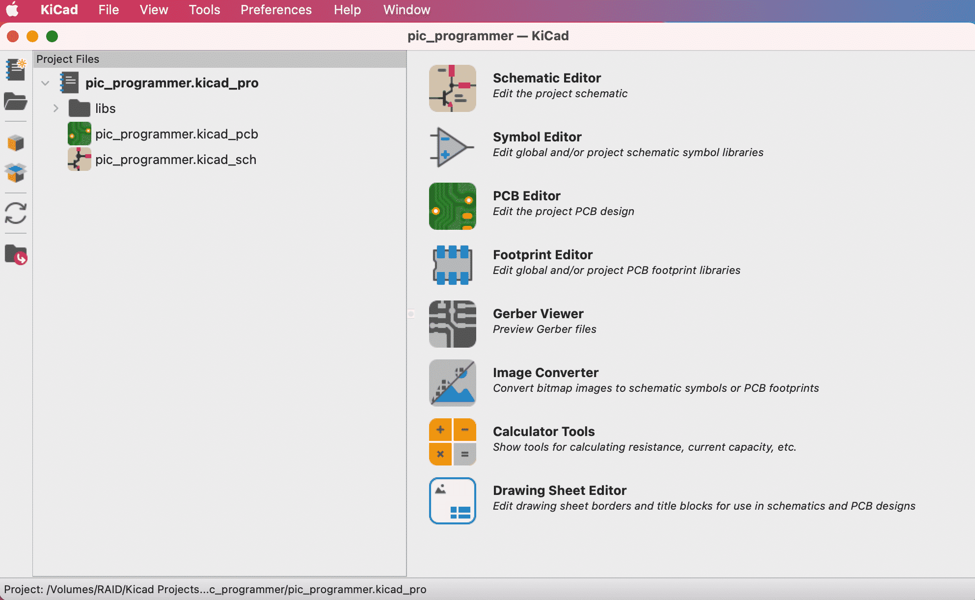
Double-click on the 'kicad_pro' (project) file. The main KiCad window will appear. This window is the launchpad for the other KiCad apps, such as the schematic editor and the layout editor. You can see the main KiCad window in Figure 1.5.2.
KiCad's schematic editor
Figure 1.5.2: The main KiCad window.
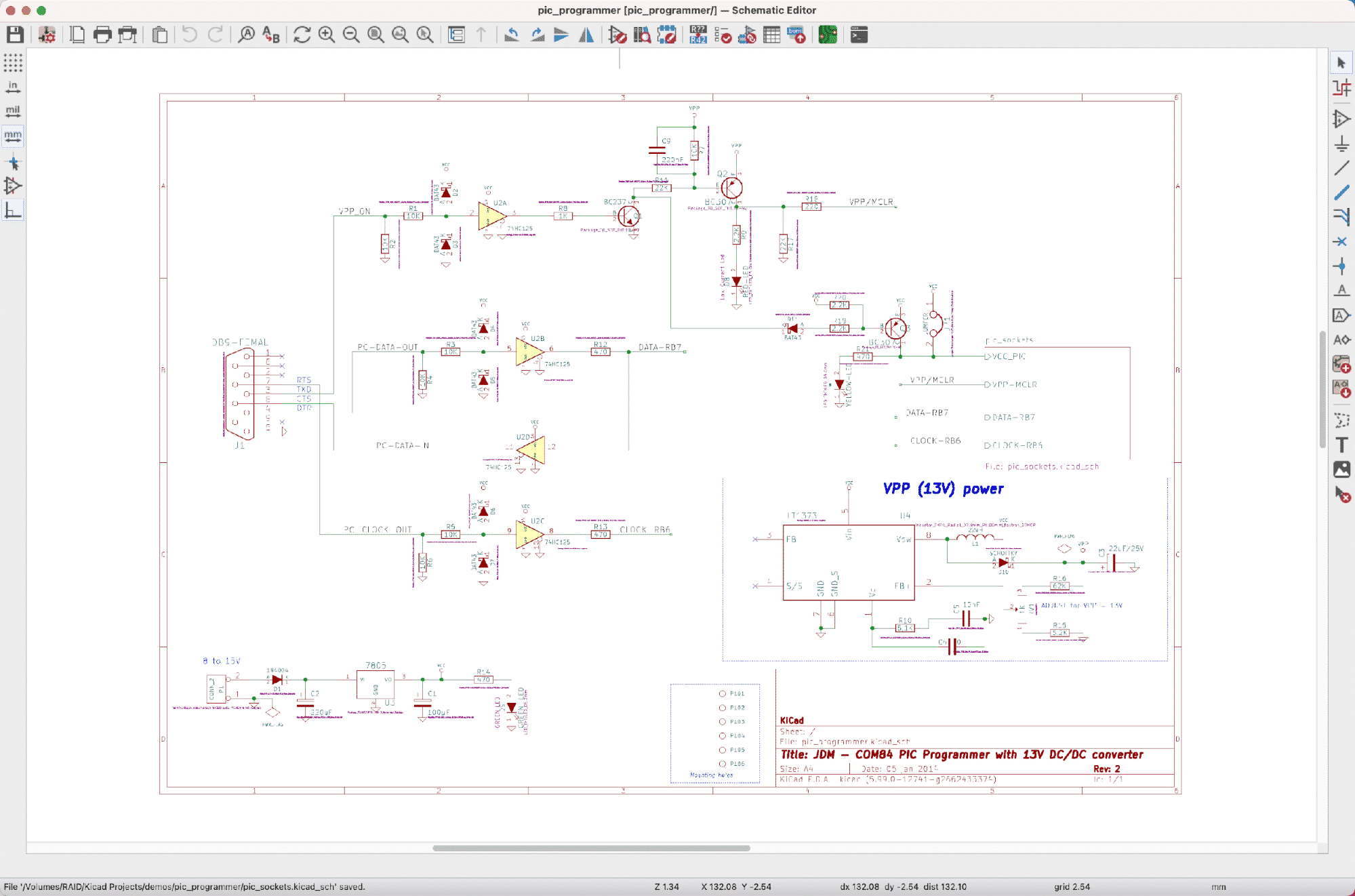
Let's explore the schematic of this demo project. The main KiCad window shows the project files in the left pane, the various app buttons in the top-right pane, and various status messages in the bottom-right pane. In the right pane, click on the Schematic Editor button. This button will start the schematic editor application, the schematic layout editor. You should see the editor as in the example in Figure 1.5.3.
Figure 1.5.3: The schematic editor.
A few things are going on here. At first, this window might seem overwhelming. Don't worry about the various buttons and menus; concentrate on the schematic itself. Look at the various symbols, like those for the diodes, the transistors, and the operational amplifiers. There are symbols for resistors and connectors, with green lines connecting their pins. Notice how text labels give names to the symbols and the wirings between pins. Notice how even the mounting holes at the bottom right side of the schematic have names. Even though these mounting holes are not electrically active, they are depicted in the schematic. The values of the capacitors and resistors are noted, and any pins that are not connected to other pins are marked with an 'x's.
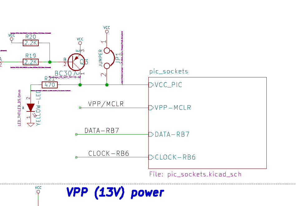
A rectangular symbol is on the schematic's right side with the title 'pic_sockets' (Figure 1.5.4).
Double-click on it. What happened?
Figure 1.5.4: A link to another sheet.
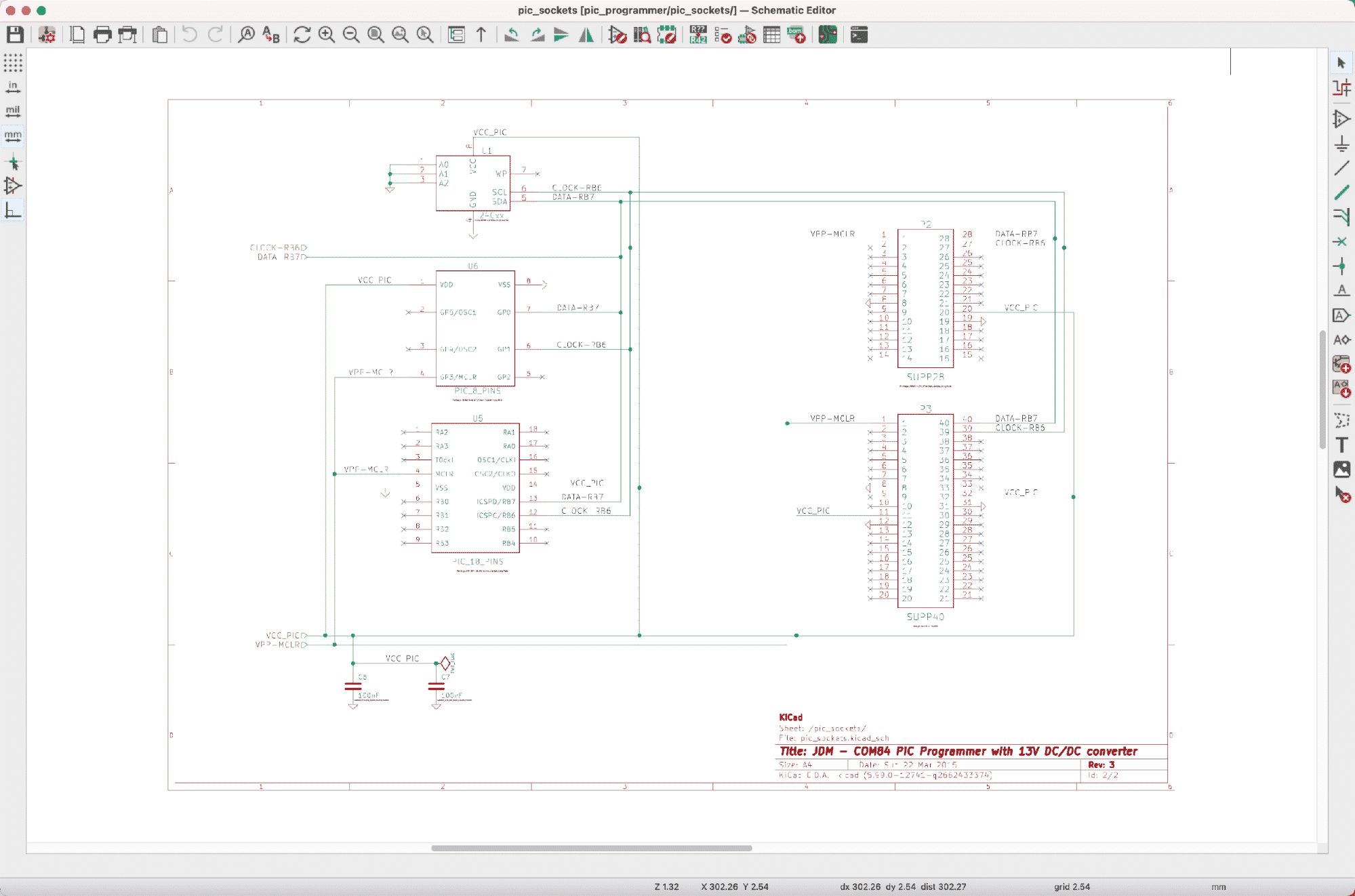
This symbol links to another sheet containing additional symbols that are part of the same schematic. It looks like the example in Figure 1.5.5.
Figure 1.5.5: KiCad’s schematics can span over multiple sheets.
KiCad's schematics can span over multiple sheets. Add more if your schematic is too large to fit in one sheet comfortably (you will learn how to do this in the KiCad Like a Pro 3e course or eBook).
I encourage you to spend a bit of time studying this schematic. You can learn a lot about drawing good schematic diagrams by studying good schematic diagrams, just like you can learn programming by studying good open-source code.
KiCad's layout editor
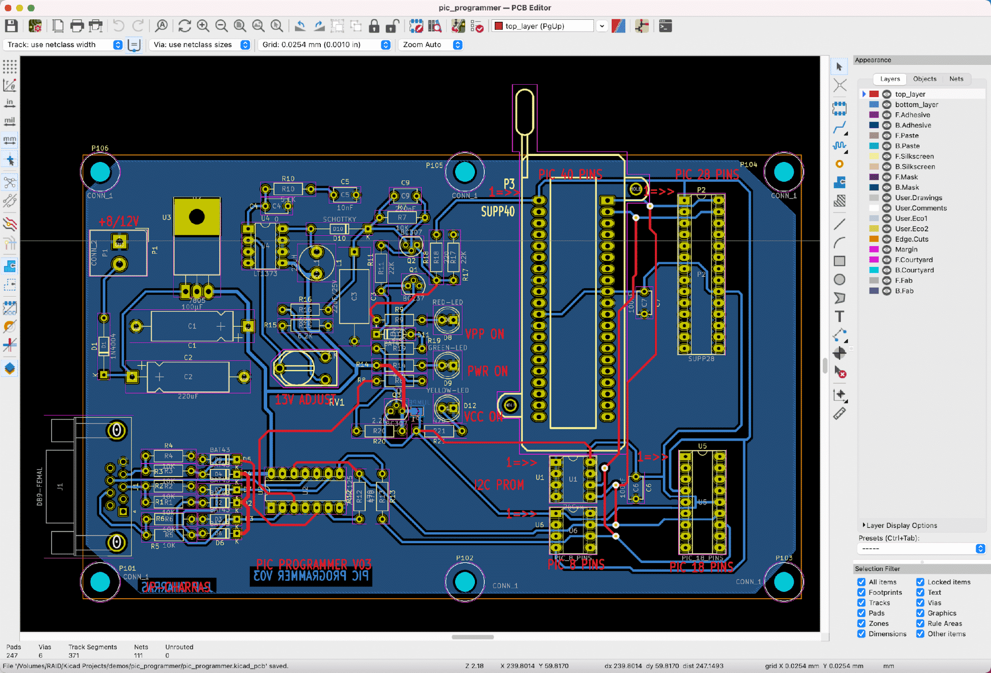
Go back to the main KiCad window. Click on the button labeled "PCB Editor." This will launch the layout editor. The window that appears will look like the example in Figure 1.5.6.
Figure 1.1.5.6: The layout editor.
Again, don't worry about the various buttons and menus; concentrate on the layout inside the sheet. Use your mouse's scroll wheel to zoom in and out and the Alt + right mouse button to pan (you should also be able to pan by holding down the middle mouse button). Zoom in and look at some of the layout details, such as the pads, how they are connected to traces, the names that appear on the pads and traces, and the colours of the front copper and back copper layer traces.
Note: in Linux, panning is done with the middle mouse button, and the Alt key is not used.
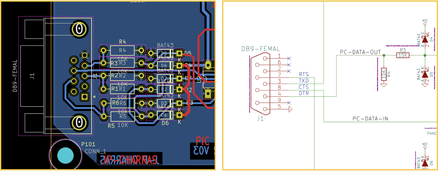
Also, compare how a footprint in the layout compares to the symbol in the schematic. You can see a side-by-side comparison in Figure 1.5.7.
Figure 1.5.7: A side-by-side comparison of a footprint (left) and its schematic symbol (right).
Associated symbols and footprints have the same designator (J1, in this example) and the same number of pins. The layout shows the traces that correspond to the wires in the schematic.
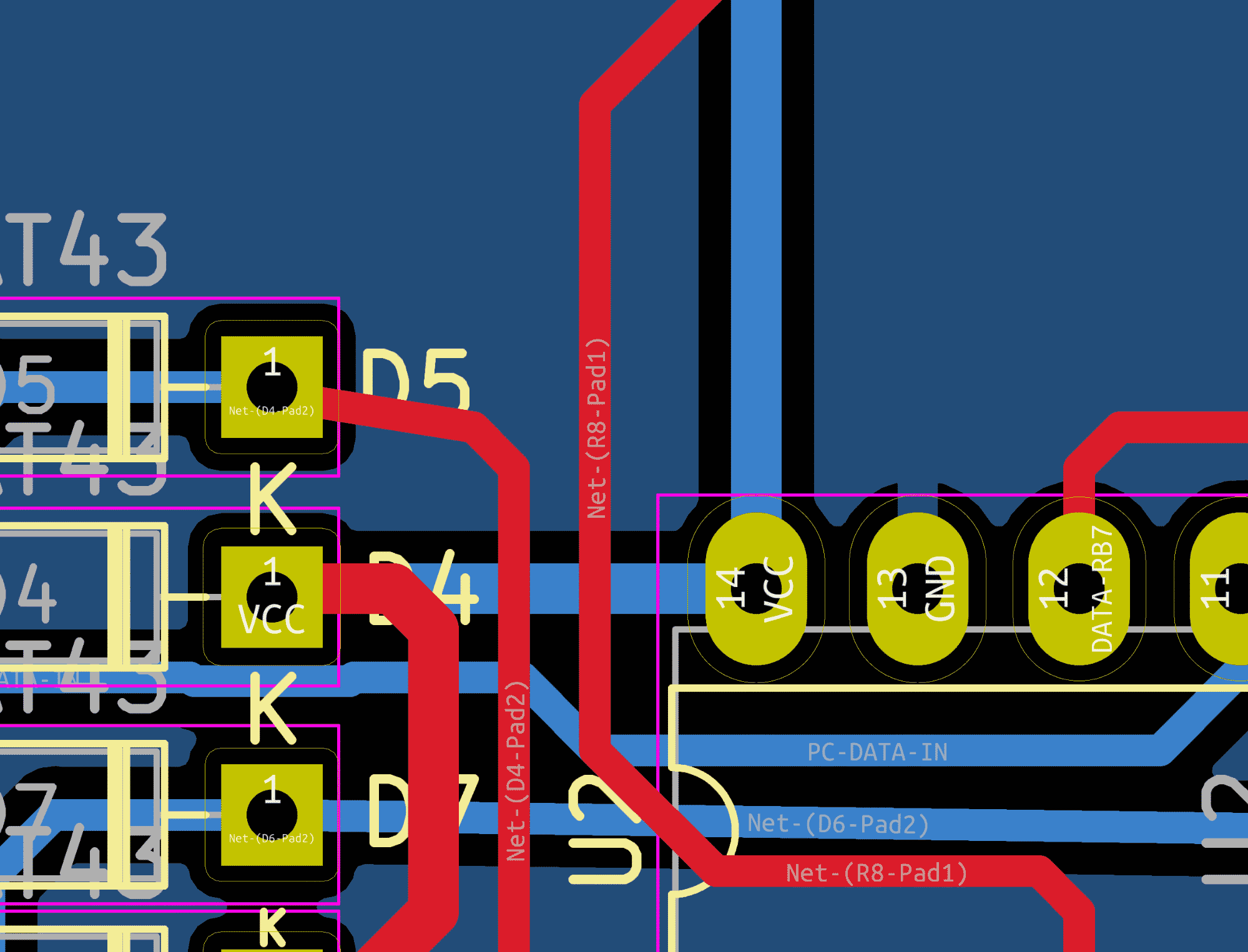
Everything you see here is configurable: the width of the traces, which layer they belong to, the shape, size, and configuration of the pads. You will learn all this in the KiCad Like a Pro 3e eBook and course. In the layout, zoom in on the J1 connector to see one of its details: the trace name that connects pad 7 of J1 to pad 1 of R5. Traces, like everything else in KiCad, have names. The names of everything that you see in the layout editor are defined (manually or automatically) in the schematic editor.
Figure 1.5.8: Traces have names.
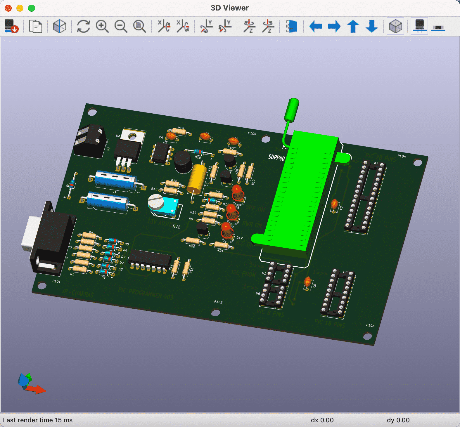
Try another thing: In the layout editor, click on the View menu and choose the 3D Viewer. The 3D Viewer will show you a three-dimensional rendering of the PCB, with remarkable detail. You can zoom in and turn the board around to see it from any angle you want (Figure 1.5.9). Many components are populated, like the LED, resistors, and some of the integrated circuits.
You can still see their pads and outlines on the board for the rest.
Figure 1.5.9: The 3D viewer will give you a realistic rendering of your board that you can examine in 3D.
As with the schematic editor, I encourage you to spend some time studying this demo project's layout. Later in the course or eBook, you will learn about the most important layout guidelines to help you design well-functioning and elegant PCBs.
Showcased KiCad projects
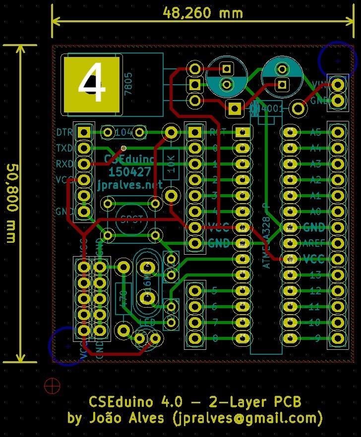
Apart from the demo projects that KiCad ships with, you should also look at some of the very impressive showcased projects of boards “made with KiCad”. For example, the CSEduino is a 2-layer PCB that contains an Atmega328P microcontroller and implements a simple Arduino clone. You will be able to easily create a board like this by the time you finish the KiCad Like a Pro 3e course or eBook. Go to txplo.re/madewkicad for more examples of projects made with KiCad.
Figure 1.5.10: Featured board 'Made with KiCad': CSEduino.
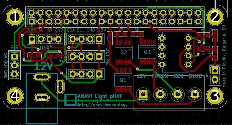
Another featured board is Anavi Light, a HAT board for the Raspberry Pi. This is also a 2-layer board that allows you to control a 12V LED strip and get readings from sensors.
Figure 1.5.11: Featured board 'Made with KiCad': Anavi Light.
Finally, a truly impressive board made with KiCad is Crazyflie (Figure 1.5.12). Crazyflie is a dense 4-layer PCB with a rather elaborate shape. The board implements the flight controller of a tiny drone. The shape is specifically designed to implement the drone's body and arms. This course and eBook will also teach you how to create complicated PCBs with complicated shapes.
Figure 1.5.12: Featured board 'Made with KiCad': Crazyflie.
With these examples, you should now understand the kinds of projects that people use KiCad. These are also the kinds of boards that you will design by the time you complete the KiCad Like a Pro 3e course or eBook. Let's get straight into the first project so that you can start discovering this fantastic tool by doing.
NextPCB’s KiCad plugin
One of the best features of KiCad is the Plugin and Content Manager (PCM). The PCM in KiCad is a feature that allows users to discover, install, and manage plugins and libraries directly within the KiCad software. It serves as a centralized repository for extending the functionality of KiCad through add-ons and content packages.
One of the most useful new plugins is the “HQ NextPCB Active Manufacturing”. You can find details on the plugin repository, and you can install it easily with the help of the PCM. Remember to add this plugin repository URL to the PCM repositories list in Tools → Plugin and Content Manager → Manage:https://raw.githubusercontent.com/HQNEXTPCB/HQNEXTPCB-kicad-addone-repository/main/repository.json
Then, install the plugin by searching for “nextpcb” (“1”, in the screenshot below) and then click “Install” (“2” in the screenshot below):
Figure 2: Installing the NextPCB plugin to KiCad.
The HQ NextPCB Active Manufacturing plugin integrates directly with KiCad, enabling you to access PCB manufacturing services from NextPCB within the KiCad environment. This plugin allows for an efficient transition from PCB design to production by providing tools to check PCB design rules, quote PCB fabrication costs, and place orders directly through NextPCB's manufacturing services.
The plugin’s key features are:
- Design Rule Check (DRC): Users can verify their PCB designs against NextPCB's manufacturing capabilities to ensure compliance with the manufacturer's specifications.
- Quotation and Ordering: The plugin provides real-time pricing for various PCB attributes such as size, layers, material, and quantity. Users can get quotes and place orders without leaving the KiCad interface.
- Seamless Integration: Designed to work within the KiCad PCB design software, streamlining the workflow from design to manufacturing.
I used the plugin with one of my KiCad Like a Pro 3e projects, and I was able to get pricing and manufacturing options without ever leaving the KiCad environment. I didn’t have to export Gerbers, upload to the NextPCB website, and repeat the process each time I wanted to make a change to the PCB. This plugin is a real time saver.
Here is how easy it is to get a quote and place an order for a PCB all within the KiCad environment using the NextPCB plugin:
Ready to learn KiCad?

Learn the world's favourite open-source PCB design tool with the world's most comprehensive course
KiCad Like a Pro, 3rd edition is available as a video course or as an eBook.
Choose the version that fits best with your style of learning, or get both to get the full benefit of the video demos plus the details of the eBook.
When you complete KiCad Like a Pro 3e, you'll be able to use KiCad to design and manufacture multi-layer PCBs with highly integrated components and a professional-looking finish.
Work through five projects that give many opportunities to learn and practice all of KiCad's important features.
KiCad Like a Pro 3e contains full sections dedicated to PCB and design principles and concepts. These ensure that you will master the fundamentals so that your PCB project are awesome.
If you are someone who is interested in designing PCBs using KiCad, or moving to KiCad from another CAD application, then KiCad Like a Pro, the video course and eBook, is for you.
Jump to another article
KiCad 6 Guides
0. Why learn KiCad?
1. What is a PCB?
2. The PCB design process
3. PCB fabrication
4. Get KiCad for your operating system
5. An example KiCad project
6. KiCad Project Manager (main window)
7. Overview of the individual KiCad apps
8. KiCad Paths and Libraries
9. Create a new KiCad project from scratch
10. Create a new KiCad project from a template
11. KiCad 6 on Mac OS, Linux, and Windows
12. Major differences between KiCad 6.0 and 5.0
13. KiCad Schematic symbols
14. PCB key terms
Contributed articles
We publish fresh content each week. Read how-to's on Arduino, ESP32, KiCad, Node-RED, drones and more. Listen to interviews. Learn about new tech with our comprehensive reviews. Get discount offers for our courses and books. Interact with our community. One email per week, no spam; unsubscribe at any time