KiCad 6 Guide series
The PCB design process
In this article I will demonstrate the technical aspects of designing a PCB in KiCad.
To design a printed circuit board, you must go through a series of steps, make decisions, and iterate until you are satisfied with the outcome. The process of creating the plans for a printed circuit board is referred to as PCB design.
Introduction
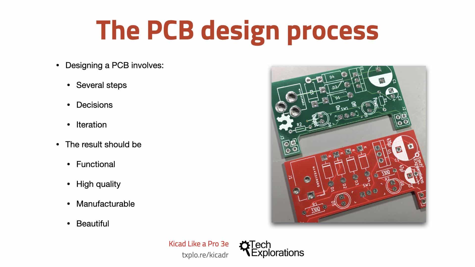
To design a printed circuit board, you have to complete several steps, make decisions, and iterate until you are satisfied with the result.
A printed circuit board is a physical device that takes time and money to manufacture. It must be fit to perform its intended purpose, and must be manufacturable. Therefore, your design must be of high quality, safe, and possible to manufacture by your chosen manufacturer.
Apart from the practical considerations of designing a PCB, there are also the aesthetic ones. You want your work to look good, not just to function well. Designing a PCB, apart from being an engineering discipline, is also a form of art.
The PCB design process

Figure 1.2.1: Some considerations of the PCB design process.
In the KiCad Like a Pro 3e course and eBook, you will learn about the technical elements of designing a PCB in KiCad, but I am sure that as you start creating your PCBs, your artistic side will emerge. Over time, your PCB will start to look uniquely yours.
PCB design is concerned with the process of creating the plans for a printed circuit board. It is different from PCB manufacturing. In PCB design, you learn about the tools, process, and guidelines useful for creating such plans.
In PCB manufacturing, on the other hand, you are concerned about the process of converting the plans of a PCB into the actual PCB.
As a designer of printed circuit boards, it is useful to know a few things about PCB manufacturing, though you surely do not need to be an expert. You need to know about the capabilities of a PCB manufacturing facility so that you can ensure that your design does not exceed those capabilities and that your PCBs are manufacturable.
As a designer, you need to have an understanding of the design process, and the design tools. To want to design PCB, I assume that you already have a working knowledge of electronics. Designing a PCB, like much else in engineering, is a procedural and iterative process that contains a significant element of personal choice. As you build up your experience and skills, you will develop your unique designing style and process.
The KiCad design workflow
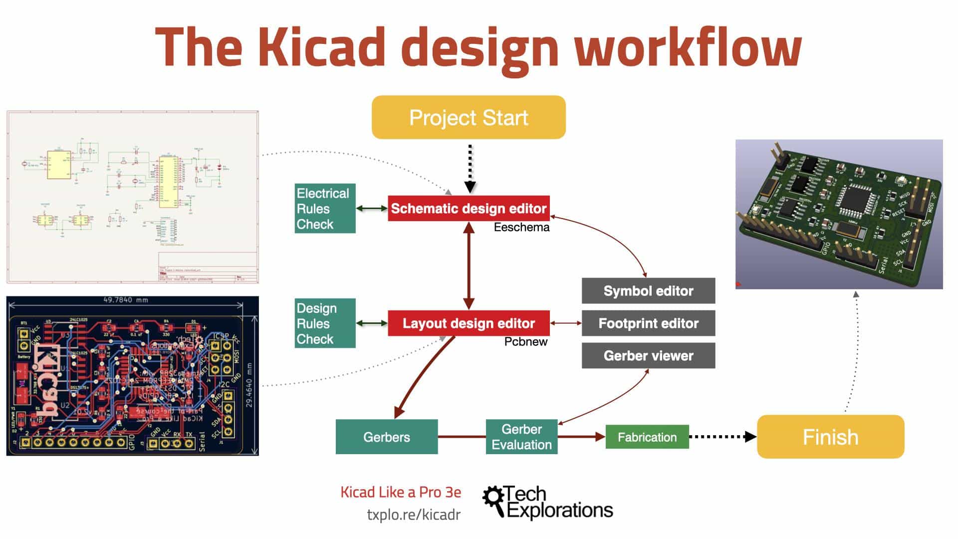
Figure 1.2.2: KiCad is a suite of applications.
KiCad is not a single application. It is a suite of apps that work together to help you create printed circuit boards. As a result, it is possible to customize the PCB design process to suit your particular style and habits. But when you are just starting up, I think it is helpful to provide a workflow that you can use as a model.
In Figure 1.2.2 you can see my KiCad PCB design workflow model. You can use it as it is, or you can modify as you see fit. I distilled this workflow by drawing from my own experience and learning from other people’s best practices. I also tried to simplify this process and make it suitable for people new to PCB design.
In the KiCad Like a Pro 3e course and eBook, I will be following this PCB design workflow in all of the projects.
From a very high-level perspective, the PCB design workflow only has two major steps:
- Step 1 is the schematic design using the schematic design editor (Eeschema);
- Step 2 is the layout design using the layout editor (Pcbnew).
Once you have the layout design, you can export it and the manufacture it.
The goal of the schematic design step is to capture information about the circuit that will be implemented in the final PCB. Once you have a schematic design, you can use the layout editor to create a version of the PCB. Remember, a schematic design can have many different layouts.
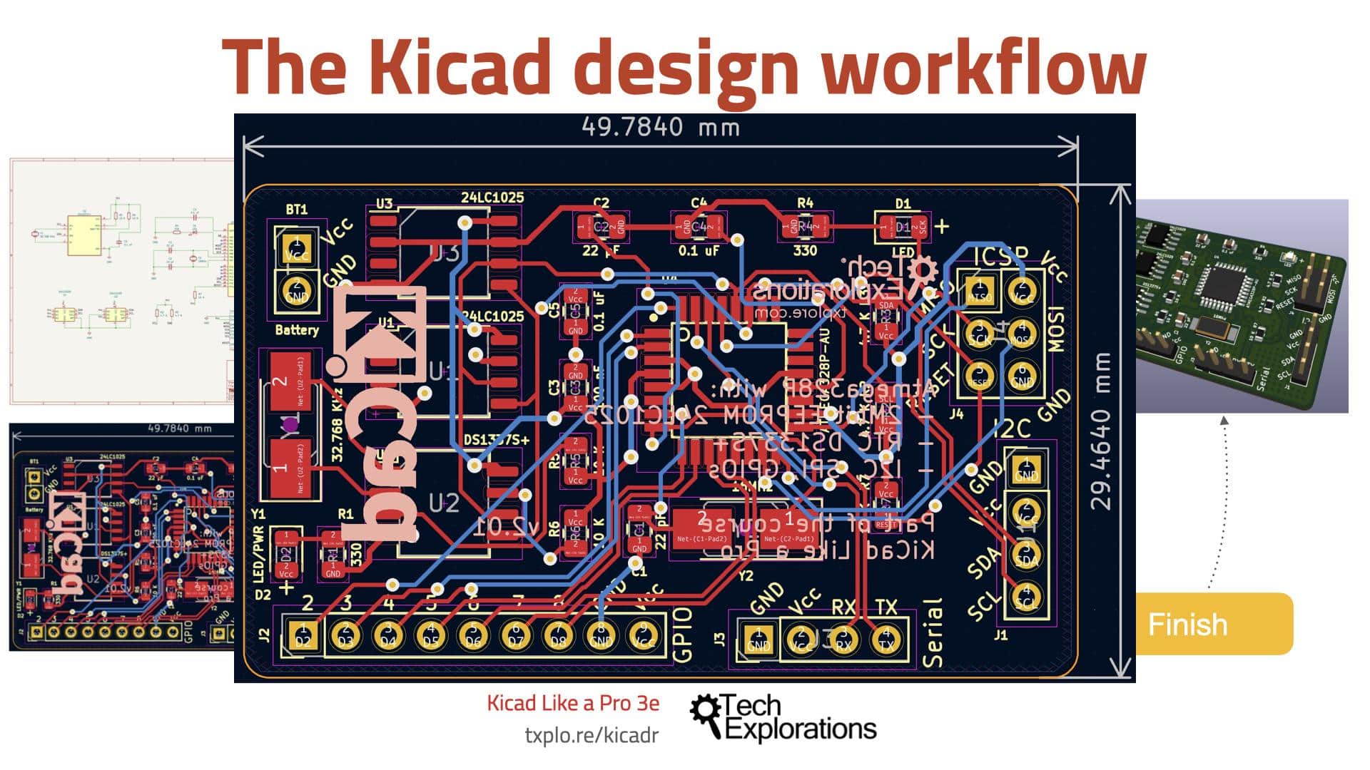
Figure 1.2.3: The KiCad layout file contains information about the physical PCB.
The KiCad layout file contains information about your board, which the manufacturer can use to create the board. The layout must contain information about the size and shape of the board; its construction (such as how many layers it must have); the location of the components on the board, the location of various board elements, like pads, holes, traces and cutouts; the features of these elements (such as the sizes of holes and traces); and much more (which you will learn in detail with the course or eBook).
Let’s walk through through the workflow now using the diagram in Figure 1.2.3 as an aid.
For the discussion that follows, keep in mind these definitions:
- A symbol is a symbolic representation of a real component in the schematic; a symbol represents a component's function, not its physical appearance or location in the final PCB.
- A footprint is a graphical depiction of a real component in the layout. It relates directly to a real physical counterpart. It contains information about the real component’s location and dimensions.
In this guide, I will be using the terms “symbols” and footprints according to the definitions above.
In KiCad, the process begins with Eeschema, which is the schematic editor.
In Eeschema you create the electrical schematic that describes the circuit that eventually will be manufactured into the PCB. You draw the schematic by selecting symbols from the library and adding them to the schematic sheet. If a component that you need doesn’t exist in the library, you can search for it on the Internet, or create yourself with the help of the schematic library editor.
Running regular electrical rules checks helps to detect defects early. Eeschema has a built-in checker utility for this purpose.
Pcbnew (KiCad's layout editor) has its own validator, the Design Rules Checker.
These two utilities help to produce PCBs that have a low risk to contain design or electrical defects.
Before you finish work in Eeschema and continue with the layout, you must first associate the schematic symbols with layout footprints.
In KiCad 6, many symbols come with preset symbol to footprint associations, but many don't, so you'll have to do this yourself. Also keep in mind that, as I said earlier, KiCad is very flexible. It is possible to assign many different footprints to the same schematic symbol (one at a time, of course).
Once you have completed the Electrical Rules Check and symbol to footprint associations, you can continue with layout using the KiCad Layout design editor, or Pcbnew.
You use Pcbnew to position the footprints on the sheet and connect the footprint pins using wires. You'll also add an outline that marks the outer limit of the PCB, and other design elements like mounting holes, logos, and instructional text.
Once you have your PCB laid out and have its traces completed, you can go ahead and do the design rules check. This check looks for defects in the board, such as a trace that is too close to a pad or two footprints overlapping.
Let's look at some of the PCB terminology before we continue.
PCB terminology
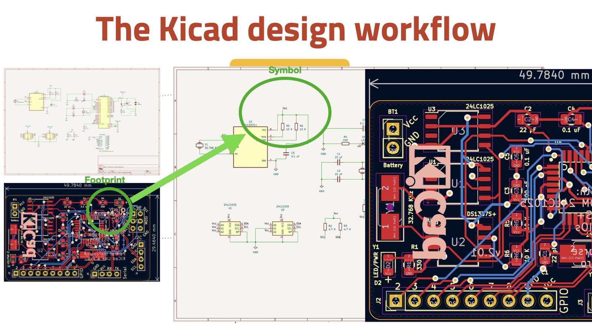
Figure 1.2.4: Symbols and footprints.
As you know, a symbol is a symbolic representation of a real component in the schematic. A footprint is a graphical depiction of a real component in the layout.
You, as the designer, must tell KiCad which footprint you want to use in your PCB by associating it to a particular symbol. Take the example of a resistor. A resistor uses a specific symbol in the schematic, but on the PCB it can be realized as a through-hole or SMD device of varying sizes.
When you are finished working on the layout, you can continue with the last step which involves exporting the layout information in a format that is compatible with your board manufacturer’s requirement.
The industry standard for this is a format called ‘Gerber.’ Gerber files contain several related files, with one Gerber file per layer on your PCB, and contain instructions that the fabrication house needs to manufacture your PCB.
Let’s move on to the next article where we’ll talk about fabrication.
Ready to learn KiCad?

Learn the world's favourite open-source PCB design tool with the world's most comprehensive course
KiCad Like a Pro, 3rd edition is available as a video course or as an eBook.
Choose the version that fits best with your style of learning, or get both to get the full benefit of the video demos plus the details of the eBook.
When you complete KiCad Like a Pro 3e, you'll be able to use KiCad to design and manufacture multi-layer PCBs with highly integrated components and a professional-looking finish.
Work through five projects that give many opportunities to learn and practice all of KiCad's important features.
KiCad Like a Pro 3e contains full sections dedicated to PCB and design principles and concepts. These ensure that you will master the fundamentals so that your PCB project are awesome.
If you are someone who is interested in designing PCBs using KiCad, or moving to KiCad from another CAD application, then KiCad Like a Pro, the video course and eBook, is for you.
Jump to another article
KiCad 6 Guides
0. Why learn KiCad?
1. What is a PCB?
2. The PCB design process
3. PCB fabrication
4. Get KiCad for your operating system
5. An example KiCad project
6. KiCad Project Manager (main window)
7. Overview of the individual KiCad apps
8. KiCad Paths and Libraries
9. Create a new KiCad project from scratch
10. Create a new KiCad project from a template
11. KiCad 6 on Mac OS, Linux, and Windows
12. Major differences between KiCad 6.0 and 5.0
13. KiCad Schematic symbols
14. PCB key terms
Contributed articles
Last Updated 1 year ago.
We publish fresh content each week. Read how-to's on Arduino, ESP32, KiCad, Node-RED, drones and more. Listen to interviews. Learn about new tech with our comprehensive reviews. Get discount offers for our courses and books. Interact with our community. One email per week, no spam; unsubscribe at any time
