KiCad 6 Guide series
PCB Fabrication
Assume you've finished laying out your board in KiCad and are ready to build it. What are your alternatives?
In this article, we will compare the benefits of making a PCB at home versus using professional PCB manufacturing services.

Make a PCB at home
Imagine that you have finished laying out your board in KiCad, and you’re ready to make it. What are your options? One option is to make your PCBs at home. There’s a guide available on the Fritzing website.
The process described in the Fritzing guide is called etching. It involves the use of various chemicals in chemical baths. Some of these chemicals are toxic. You have to have special safety equipment and keep your children and pets away. The process emits smelly and potentially dangerous fumes. Once you have your board etched, you still need to use a drill to make holes and vias and then figure out how to connect your top and bottom layers.
Professional PCB manufacturing services
If this sounds like not your kind of thing (I’m with you!), then you can opt for a professional PCB manufacturer service. PCBWay, NextPCB, and OSH Park are very good at what they offer.
You can get a professionally made PCB for around $15 for several copies and without danger to yourself as well. I’ve used OSHPark (great for beginners thanks to its straightforward user interface) and PCBWay (great for more advanced projects that need an extensive array of manufacturing options) extensively. I’m always happy with the result. Using an online manufacturer takes a little bit of planning because once you order your PCBs, it can take up to several weeks to be delivered. If you’re in a hurry, there are options to expedite the process if you are willing to pay a premium.
The typical small standard two-layer order costs around $10 for a two square inch board; you get three copies of that. This price works out to around $5 per square inch. The pricing is consistent in the industry, where the main cost factor is the size of the PCB. There is a strong incentive to make your PCBs as small as possible. Be aware of this when you design your layout.
What is a Gerber file

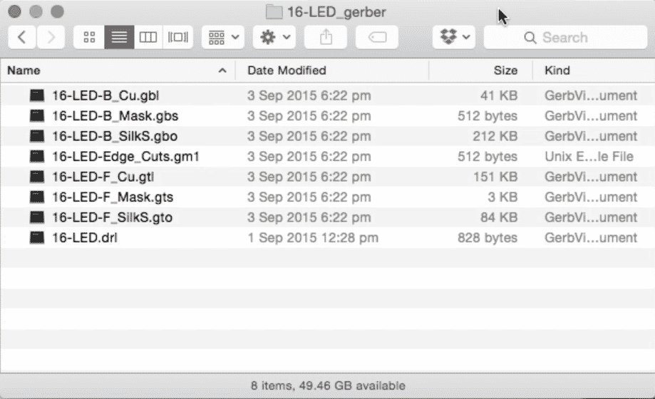
Figure 3.3.1: An example of the Gerber files that the manufacturer will need in order to make your PCB.
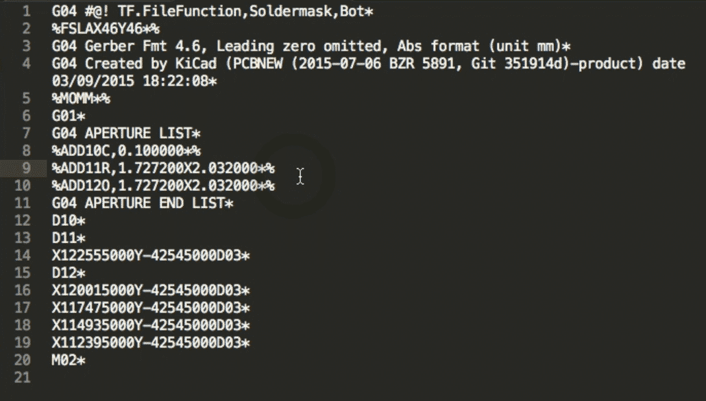
Now, let’s turn our attention to the files you need to upload for these services — and the files are Gerber files. Each layer on your PCB has its own Gerber file, which is simply a text file. Figure 3.3.2 shows the contents of an example Gerber file.

Figure 3.3.3: Gerber files contain text
You can see that this is just a text-based file that contains instructions. An advantage of this text format is that you can use a version control system like Git to maintain your project history and store and share via online repositories like Github.
Ucamco has designed the Gerber files system and standard. They make equipment and write software for PCB manufacturers — things like PreCAM software, PCB CAM, laser photoplotters, and direct imaging systems. If you’re curious about how to read these Gerber files, you can look up the Gerber format specification on Ucamco’s website.
Ready to learn KiCad?

Learn the world's favourite open-source PCB design tool with the world's most comprehensive course
KiCad Like a Pro, is available as a video course or as an eBook.
Choose the version that fits best with your style of learning, or get both to get the full benefit of the video demos plus the details of the eBook.
When you complete KiCad Like a Pro, you'll be able to use KiCad to design and manufacture multi-layer PCBs with highly integrated components and a professional-looking finish.
Work through five projects that give many opportunities to learn and practice all of KiCad's important features.
KiCad Like a Pro contains full sections dedicated to PCB and design principles and concepts. These ensure that you will master the fundamentals so that your PCB project are awesome.
If you are someone who is interested in designing PCBs using KiCad, or moving to KiCad from another CAD application, then KiCad Like a Pro, the video course and eBook, is for you.
Jump to another article
KiCad 6 Guides
0. Why learn KiCad?
1. What is a PCB?
2. The PCB design process
3. PCB fabrication
4. Get KiCad for your operating system
5. An example KiCad project
6. KiCad Project Manager (main window)
7. Overview of the individual KiCad apps
8. KiCad Paths and Libraries
9. Create a new KiCad project from scratch
10. Create a new KiCad project from a template
11. KiCad 6 on Mac OS, Linux, and Windows
12. Major differences between KiCad 6.0 and 5.0
13. KiCad Schematic symbols
14. PCB key terms
Contributed articles
Last Updated 1 year ago.
We publish fresh content each week. Read how-to's on Arduino, ESP32, KiCad, Node-RED, drones and more. Listen to interviews. Learn about new tech with our comprehensive reviews. Get discount offers for our courses and books. Interact with our community. One email per week, no spam; unsubscribe at any time
