In the previous articles of this guide series, you learned about some of KiCad's most commonly used features. You used Eeschema and Pcbnew to design the schematic diagram and the layout of a simple board. You also had your first experience with some of the decisions a PCB designer must make during a printed circuit board design process.
Before you continue your learning journey with more interesting PCB projects, it is appropriate to become familiar with concepts, conventions, and design patterns that will help you work and produce better-performing boards.
You will learn about the symbols and units that appear in the schematic diagrams and the layout diagrams.
You will also learn the terminology used to describe a printed circuit board's various components and characteristics.
In Part six of the KiCad Like a Pro 3e course and eBook, you can learn about the general processes of the schematic and layout steps of designing a PCB. These are processes that every designer will go through to one degree or another, regardless of which CAD application they are using.
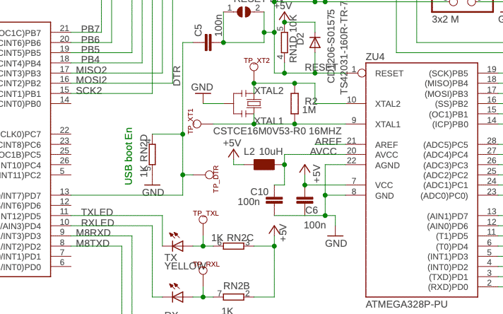
Electronics and PCB design has their own symbolic language. We use this language to create schematic diagrams. In Figure 5.2.1 you can see an example of a schematic that contains several symbols of this language.
This example shows the schematic symbols of several components that make up the Arduino Uno Rev3. The large rectangular symbol with the designator 'ZU4' is the ATMEGA328P-PU microcontroller chip. The symbol contains several pins that provide inputs and outputs, and each of them is named.
You can see a few capacitors, designated C5, C10, and C6, none of them polarized. There is one resistor, R2, and a few resistor networks (like RN2 and RN1, which are simple resistors in a network configuration). The capacitors and the resistor also have their values marked in the schematic. There are also symbols for an LED, a jumper connector, and power (Vcc, RAW, and GND).
All of these symbols follow a particular standard. . Several standards are available, but most notably, engineers worldwide tend to work with the American style ('IEEE') or the European ('IEC') style. The symbols in Figure 5.2.1 follow the IEC style.
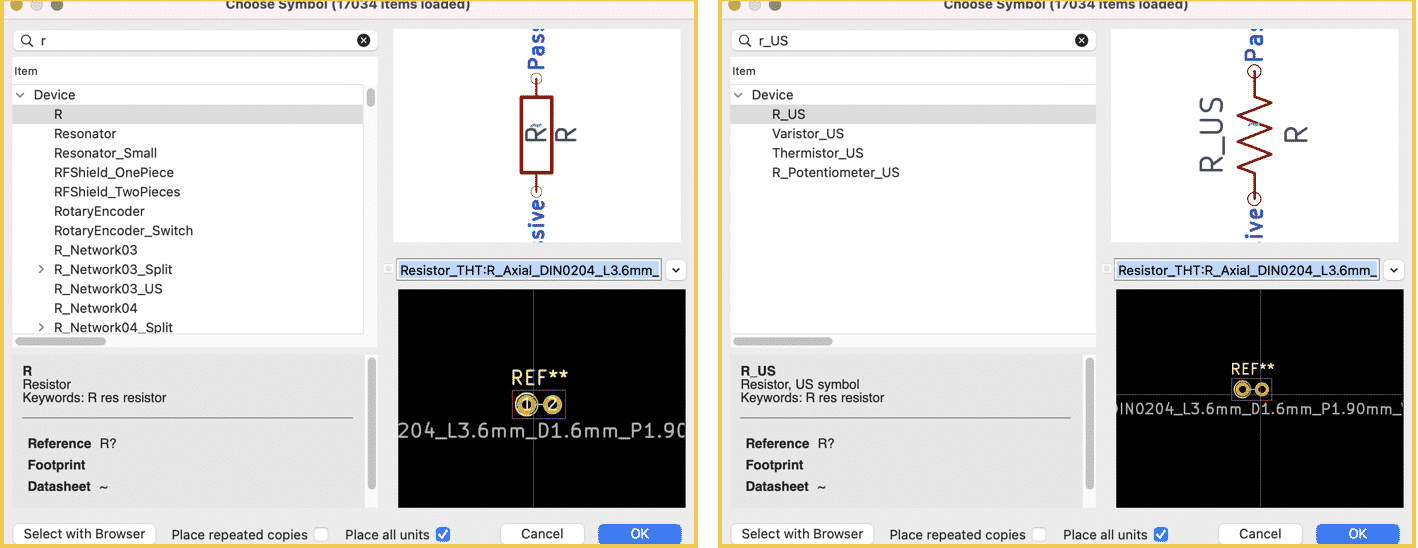
In KiCad, you can choose to use either the American or the European style symbols. Whichever one you choose, be consistent. Do not mix American-style resistor symbols with European-style capacitor symbols in the same schematic.
The KiCad standard symbols library contains symbols of both styles, though the European symbols seem more plentiful. In most cases, American-style symbols will have the postfix 'US' in their name. In Figure 5.2.2, you can see an example of a resistor symbol, with the European style on the left and the American on the right. The name of the American-style symbol ends in 'US,' and you can take that into account when you are searching for a symbol in the Symbol Chooser (Figure 5.2.2).


